5V-2
!PWM DRIVE
; 0701 0702
I
l
12V
..,
>
~
>
TP20ll
V. DRIVE
NTC
12V
TP2012
NTC
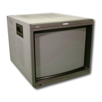
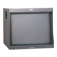
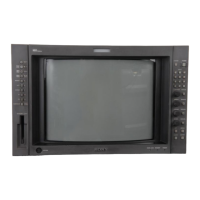
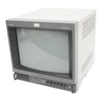
20 inch
-12v
RfTRACE 15V
BOOST SW
D606,D607
CN500012/21
18a E-PROT
19a POWER. ON
14a AFC.P
9a V.BLK.PI
80 V, BLK. P2
8b H. BLK, P
60 Ml SO
H, DY V.DY
r- --- --- - -- - -- - -- - - --- -- ---- - - - - - - -- - -- - --- -
---------------~
I
I
I
I
12V
l '------r ........... /----"~~~:::~~:::;'t,... ..... --!----.l---J;;;:t.nT--i--,-r,.......,.
I
I
I
I
I
I
I TP2014
I
JH,CONV,C
TP2015
H. CONY. SIDE
3-17
-12V
12V
RETRACE BOOST SW
0301
I
I
I
I
I
I
I
I
I
I
I
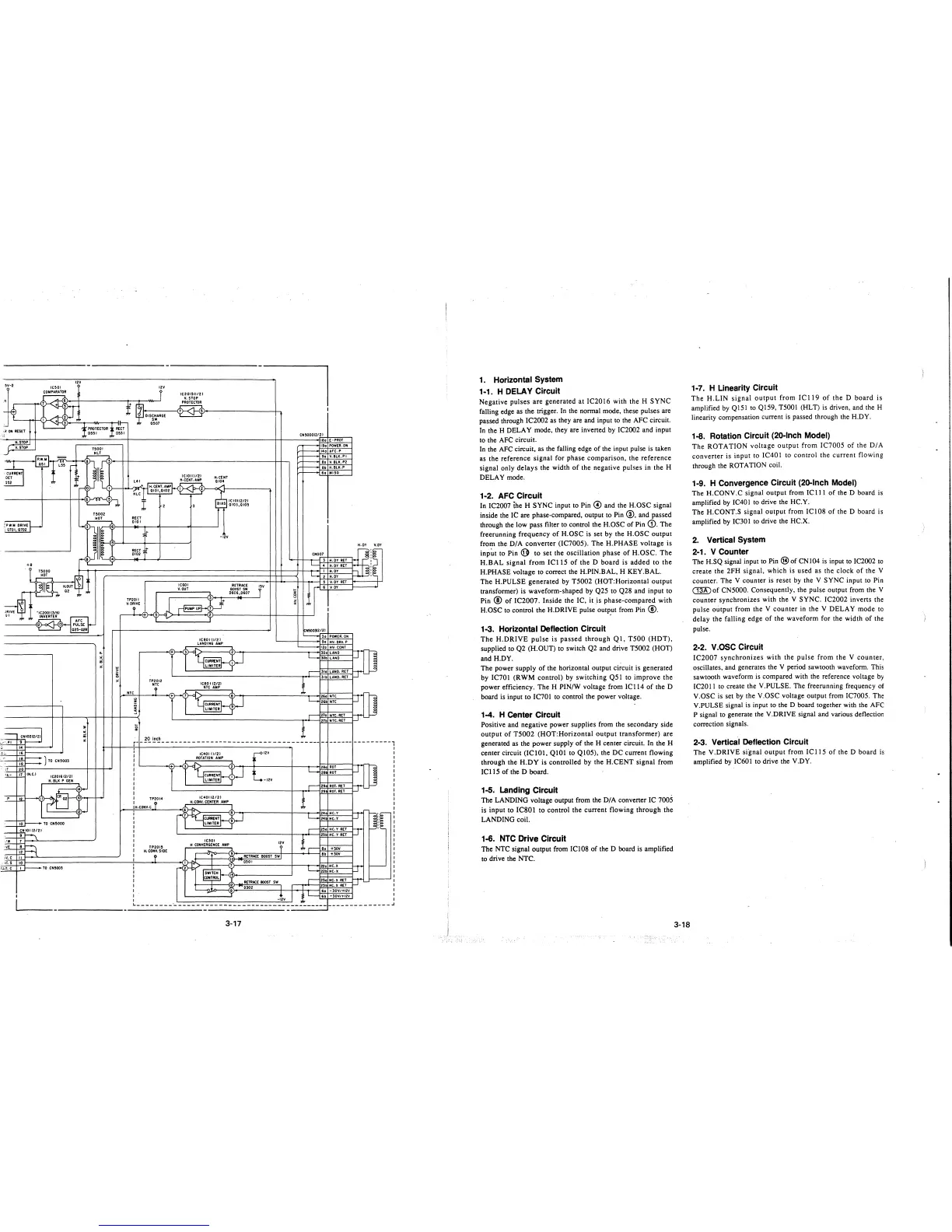
1. Horizontal System
1-1. H DELAY Circuit
Negative pulses are generated at IC2016 with the H SYNC
falling edge as the trigger. In the normal mode, these pulses are
passed through IC2002 as they are and input to the AFC circuit.
In the H DELAY mode, they are inverted by IC2002 and input
to the AFC circuit.
In the AFC circuit, as the falling edge of the input pulse is taken
as the reference signal for phase comparison, the reference
signal only delays the width of the negative pulses in the H
DELAY mode.
1-2. AFC Circuit
In IC2007 the H SYNC input to Pin @ and the H.OSC signal
inside the IC are phase-compared, output to Pin
@, and passed
through the low pass filter to control the H.OSC of Pin
G). The
freerunning frequency of H.OSC is set by the H.OSC output
from the
DIA converter (IC7005). The H.PHASE voltage is
inp~t to Pin G) to set the oscillation phase of H.OSC. The
H.BAL signal from IC! 15 of the D board is added to the
H.PHASE voltage
to correct the H.PIN.BAL, H KEY.BAL.
The H.PULSE generated by T5002 (HOT:Horizontal output
transformer) is waveform-shaped by Q25 to Q28 and input to
Pin @ of IC2007. Inside the IC, it is phase-compared with
H.OSC to control the H.DRIVE pulse outp,ut from Pin @.
1-3. Horizontal Deflection Circuit
The H.DRIVE pulse is passed through QI, T500 (HOT),
supplied to Q2 (H.OUT) to switch Q2 and drive T5002 (HOT)
and H.DY .
The power supply of the horizontal output circuit is generated
by IC701
(RWM control) by switching Q51 to improve the
power efficiency. The H PIN/W voltage from ICl 14 of the D
board is input to IC701 to control the power voltage.
1-4. H Center Circuit
Positive and negative power supplies from the secondary side
output of T5002 (HOT:Horizontal output transformer) are
generated as the power supply of the H center circuit. In the H
center circuit (IClOl, QIOl to Q105), the DC current flowing
through the H.DY is controlled by the H.CENT signal from
ICl 15 of the D board.
1-5. Landing Circuit
The LANDING voltage output from the D/A converter IC 7005
is input to IC801 to control the current flowing through the
LANDING coil.
1-6. NTC Drive Circuit
The NTC signal output from IC108 of the D board is amplified
to drive the NTC.
3-18
1-7. H Linearity Circuit
The H.LIN signal output from ICl 19 of the D board is
amplified by Q151 to Q!59, T5001 (HLT) is driven, and the H
linearity compensation current is passed through the H.DY.
1-8. Rotation Circuit (20-lnch Model)
The ROTATION voltage output from IC7005 of the D/A
converter is input to IC401 to control the current flowing
through the ROTATION coil.
1-9. H Convergence Circuit (20-lnch Model)
The H.CONV.C signal output from ICl 11 of the D board is
amplified by IC401 to drive the HC.Y.
The H.CONT.S signal output from ICI08 of the D board is
amplified by IC301 to drive the HC.X.
2. Vertical System
2-1. V Counter
The H.SQ signal input to Pin @ of CNI04 is input to IC2002 to
create the 2FH signal, which is used as the clock of the V
counter. The V counter is reset by the V SYNC input to Pin
QIDof CN5000. Consequently, the pulse output from the V
counter synchronizes with the
V SYNC. IC2002 inverts the
pulse output from the V counter in the V DELAY mode to
delay the falling edge of the waveform for the width of the
pulse.
2-2. V .OSC Circuit
IC2007 synchronizes with the pulse from the V counter,
oscillates, and generates the V period sawtooth waveform. This
sawtooth waveform is compared with the reference voltage by
IC201 I to create the V.PULSE. The freerunning frequency of
V .OSC is set by the V .OSC voltage output from IC7005. The
V.PULSE signal is input to the D board together with the AFC
P signal to generate the V.DRIVE signal and various deflection
correction signals.
2-3. Vertical Deflection Circuit
The V.DRIVE signal output from IC! 15 of the D board is
amplified by IC601 to drive the V.DY.
 Loading...