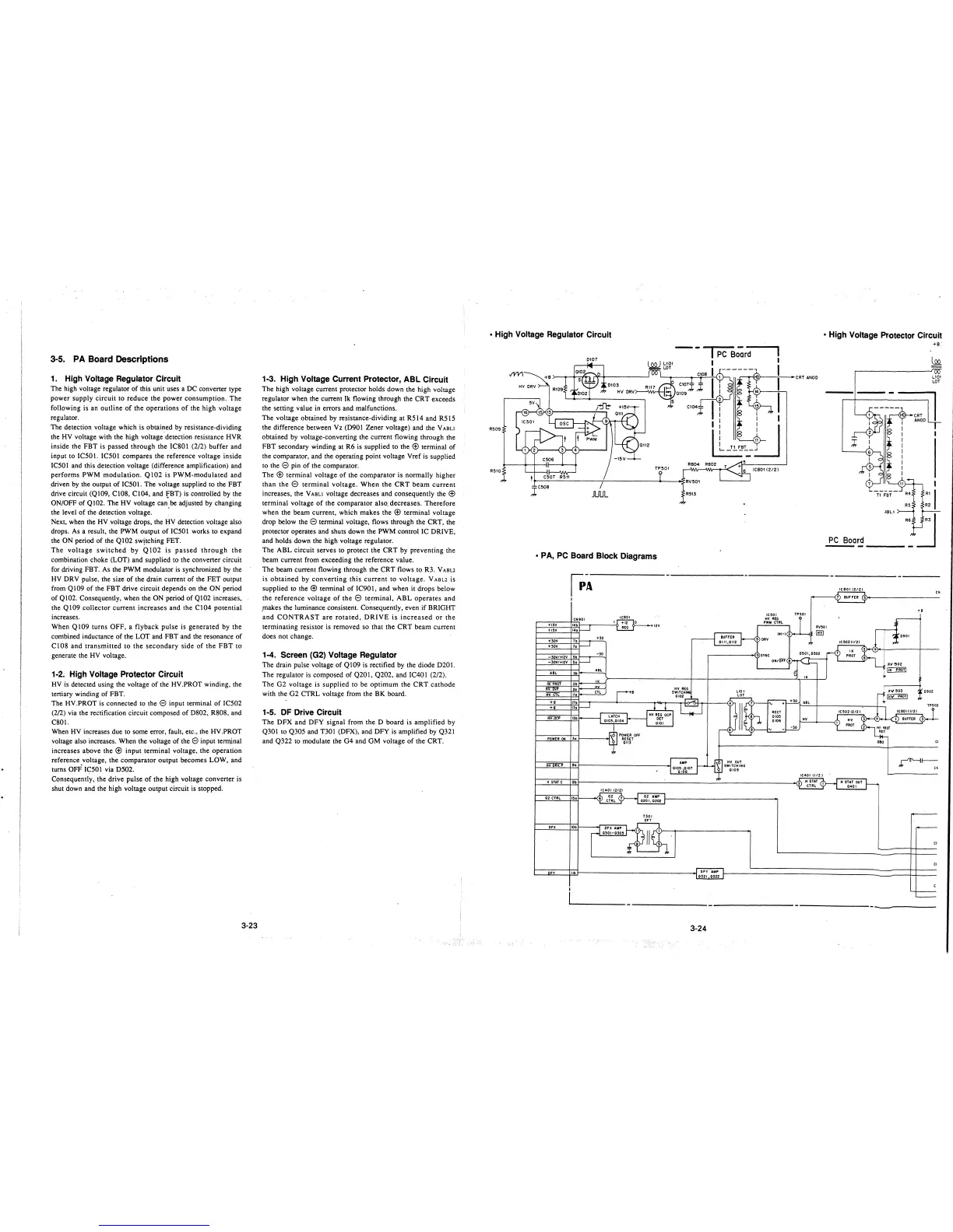
3-5. PA Board Descriptions
1. High Voltage Regulator Circuit
The high voltage regulator of this unit uses a DC converter type
power supply circuit to reduce the power consumption. The
following is an outline of the operations of the high voltage
regulator.
The detection voltage which is
obtai~ed by resistance-dividing
the HY voltage with the high voltage detection resistance HYR
inside the FBT is passed through the IC801 (2/2) buffer and
input to IC50l. IC501 compares the reference voltage inside
IC501 and this detection voltage (difference amplification) and
performs PWM modulation. Ql02 is PWM-modulated and
_driven by the output of IC501. The voltage supplied to the FBT
drive circuit (Q109, C108, Cl04, and
1_:BT) is controlled by the
ON/OFF of Q102. The HY voltage can.be adjusted by changing
the level of the detection voltage.
Next, when the HY voltage drops, the HY detection voltage
also
drops. As a result, the PWM output of IC501 works to expand
the ON period of the Q102 switching FET.
The voltage switched by Ql02 is passed through the
combination choke (LOT) and supplied to the converter circuit
for driving FBT. As the PWM modulator is synchronize.cl by the
HY DRY pulse, the size of the drain current of the FET output
from Ql09 of the FBT drive circuit depends on the ON period
of Ql02. Consequently, when the ON period of Q102 increases,
the Ql09
.. collector current increases and the C104 potential
increases.
When Q109 turns OFF, a flyback pulse is generated by the
combined inductance of the LOT and FBT and the resonance of
C108 and transmitted to the secondary side of the FBT to
generate the HY voltage.
1-2~ High Voltage Protector Circuit
HY is detected using the voltage of the HY.PROT winding, the
tertiary winding of FBT.
The HY.PROT is connected to the
8 input terminal of IC502
(2/2) via the rectification circuit composed of D802, R808, and
C80l.
When HY increases due to some error, fault, etc., the HY.PROT
voltage also increases. When the voltage of the
8 input termjnal
increases above the Et> input terminal voltage, the operation
reference _voltage, the comparator output becomes LOW, and
turns OFF IC501 via D502.
Consequently, the drive pulse of the high voltage converter is
shut down and the high voltage output circuit is stopped.
3-23
1-3. High Voltage Current Protector, ABL Circuit
The high voltage current protector holds down the high voltage
regulator when the current Ik flowing through the CRT exceeds
the setting value in errors and malfunctions.
The voltage obtained by resistance-dividing at R5 l 4 and R5 l 5
the difference between Yz (D901 Zener voltage) and the
YABLI
obtained by voltage-converting the current flowing through the
FBT secondary winding at R6 is supplied to the
Et> terminal of
the comparator, and the operating point voltage Yref is supplied
to the
e pin of the comparator.
The
Et> terminal voltage of the comparator is normally higher
than the
8 terminal voltage. When the CRT beam current
increases, the Y
ABLI voltage decreases and consequently the Et)
terminal voltage of the comparator also. decreases. Therefore
when the beam current, which makes the
Et> terminal voltage
drop below thee terminal voltage, flows through the CRT, the
protector operates and shuts down the PWM control IC DRIVE,
and holds down the high voltage regulator.
The ABL circuit serves to protect the CRT by preventing the
beam current from exceeding the reference value.
The beam current flowing through the CRT flows to R3. V
ABL2
is obtained by converting this current to voltage. Y ABL2 is
supplied to the
Et> terminal of IC901, and when it drops below
the reference voltage of the
8 te_rminal, ABL operates and
.makes the luminance consistent. Consequently, even if BRIGHT
and CONTRAST are rotated, DRIVE is increased or the
terminating resistor is removed so that the CRT beam current
does not change.
1-4. Screen (G2) Voltage Regulator
The drain pulse voltage of Q109 is rectified by the diode D201.
The regulator is composed of Q201, Q202, and IC401 (2/2).
The
02 voltage is supplied to be optimum the CRT cathode
with the G2 CTRL voltage from the
BK board.
1-5. OF Drive Circuit
The DFX and DFY signal from the D board is amplified by
Q301 to Q305 and T301 (DFX), and DFY is amplified by Q321
and Q322 to modulate the G4 and GM voltage of the CRT.
• High Voltage Regulator Circuit
RS09
RS10
0107
I
JlfiJL
TPSOI
• PA, PC Board Block Diagrams
+i,v
-tl!5Y
+30Y
T30V
-30Vl+12V
-30Y/+12V
&BL
IK PROT
RnvP
iii'cTL'
+a
+a
iiv:6CP
POWER ON
7b
7a
5b
5a
3b
2b
2a
Ila
17b
17a
15b
3a
IC901
POWER OFF
RESET
0113
------
PC Boord
RS13
iinli'l1'
a,
!!:=J]:~------------1 AMP
0105 ,0107
QIOB
HY OUT
SWITCHING
0109
H STAT C
G2 CTRL
DFX
Sb
IOb
G2 AMP
020,. 0202
T301
OFT
ICB0112/2l
TP501
• High Voltage Protector Circuit
PC Board
H STAT OUT
0401
+e:
UlQ_
=
___ :_~
~~~1011
+a
D901
081!
Cl
Cl
Cl
t
=:iE.it:=:::::Jii111iJ------------------r DFY AMP
0321 0322 r-----------------------+-4--
3-24
 Loading...