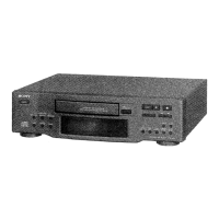
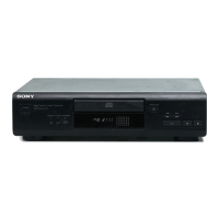
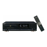
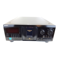
CDP-M11/M12/M21/M41
SAFETY-RELATED
COMPONENT
WARNING!!
COMPONENTS
IDENTIFIED
BY
MARK
AX
OR
DOTTED
LINE
WITH
MARK
AX
ON
THE
SCHEMATIC
DIAGRAMS
AND
IN
THE
PARTS
LIST
ARE
CRITICAL
TO
SAFE
OPERATION.
REPLACE
THESE
COMPONENTS
WITH
SONY
PARTS
WHOSE
PART
NUMBERS
APPEAR
AS
SHOWN
IN
THIS
MANUAL
OR
IN
SUPPLEMENTS
PUBLISHED
BY
SONY.
PROTECTION
OF
EYES
FROM
LASER
BEAM
DURING
SERVICING
This
set
employs
a
laser.
Therefore,
be
sure
to
follow
carefully
the
instructions
below
when
servicing.
CAUTION
Use
of
controls
or
adjustments
or
performance
of
procedures
other
than
those
specified
herein
may
result
in
hazardous
radiation
exposure.
NOTES
ON
HANDLING
THE
OPTICAL
PICK-UP
BLOCK
OR
BASE
UNIT
The
laser
diode
in
the
optical
pick-up
block
may
suffer
electrostatic
breakdown
because
of
the
potential
difference
generated
by
the
charged
electrostatic
load,
etc.
on
clothing
and
the
human
body.
During
repair,
pay
attention
to
electrostatic
breakdown
and
also
use
the
procedure
in
the
printed
matter
which
is
included
in
the
repair
parts.
The
flexible
board
is
easily
damaged
and
should
be
handled
with
care,
Laser
Diode
Properties
¢
Material:
GaAlAs
¢
Wavelength:
780nm
¢
Emission
Duration:
continuous
e
Laser
Output:
max.44.6.W*
*
This
output
is
the
value
measured
at
a
distance
of
about
200mm
from
the
objective
lens
surface
on
the
Optical
Pick-up
Block.
During
service,
do
not
take
the
Optical
Pick-up
Block
apart,
and
do
not
adjust
the
APC
circuit.
If
there
is
a
breakdown
in
the
APC
circuit
(including
laser
diode),
replace
the
entire
Optical
Pick-
up
Block
(including
APC
borad).
TABLE
OF
CONTENTS
Section
Title
Page
1.
GENERAL
wie
seccccstssersccnccnccenemsnsnecsconsonsonsens
4
41-1.
Location
of
Controls
.........
ce
eescsseseeseeeesenenee
4
1-2
Pir)
FUNCTION
ou...
eceece
coset
neeeeseneeeneneesnneeee
5
2.
ELECTRICAL
BLOCK
CHECKING
...........00
7
3.
DISASSEMBLY
..0.......cccessesccsssececssnncnensccnneesessns
9
4.
DIAGRAMS.
..u........csscscecesesseesecnereeeenessneensnsnonnnsees
10
Section
4-1.
Block
Diagrams
4-2.
Waveforms
4-3.
Printed
Wiring
Boards
...........c:seseeseeereseenes
14
4-4.
Schematic
diaGram
........csesecereeeeeseeereereeasees
17
4-5.
Semiconductor
Lead
Layout
......----:seseee
21
4-6.
IC
Block
Diagrams
ou...
esceeesereernetetenetenenenes
22
EXPLODED
VIEWS.
...........:csssssssecsseenenesssersenes
24
ELECTRICAL
PARTS
LIST
.......::cssssesnsesssssseses
27