– 43 – – 44 –
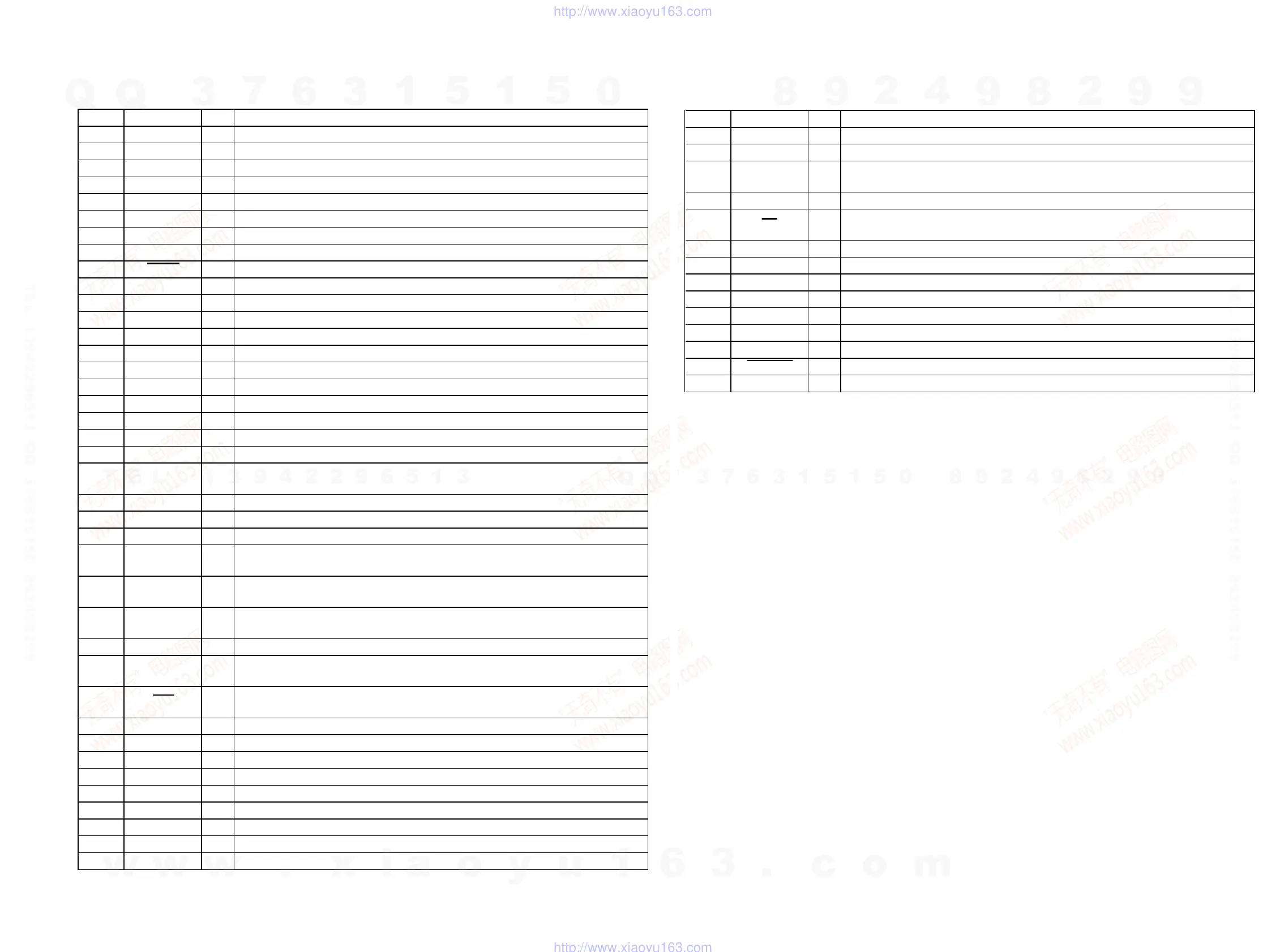
• LCD BOARD IC501 CXP83620-011Q (SYSTEM CONTROLLER)
Pin No. Pin Name I/O Description
1 C-SCOR I Subcode sync (S0+S1) detection signal input from the CXD2589Q (IC703)
2 RMC I Sircs remote control signal input terminal Not used (fixed at “L”)
3 BUZZER O Buzzer sound signal output terminal
4 LED O LED drive signal output of the ALARM indicator (D602) “L”: LED on
5 C-SENS I Internal status signal (sense signal) input from the CXD2589Q (IC703)
6 C-SENS2 I Internal status signal (sense signal) input from the CXA1992BR (IC701)
7 C-SQCK O Subcode Q data reading clock signal output to the CXD2589Q (IC703)
8 C-SQSO I Subcode Q data input from the CXD2589Q (IC703)
9 C-RST O System reset signal output to the CXA1992BR (IC701) and CXD2589Q (IC703) “L”: reset
10 C-CLOCK O Serial data transfer clock signal output to the CXD2589Q (IC703)
11 C-LATCH O Serial data latch pulse signal output to the CXD2589Q (IC703)
12 C-DATA O Serial data output to the CXD2589Q (IC703)
13 REC I Record/playback detection signal input terminal “L”: recording mode, “H”: playback mode
14 R-COUNT I PLL serial data input from the FM/AM PLL (IC2)
15 R-DATA O PLL serial data output to the FM/AM PLL (IC2)
16 R-CLOCK O PLL serial data transfer clock signal output to the FM/AM PLL (IC2)
17 R-LATCH O PLL serial data latch pulse signal output to the FM/AM PLL (IC2)
18 V-LATCH O
Serial data latch pulse signal output to the electrical volume (IC302)
19 V-DATA O
Serial data output to the electrical volume (IC302)
20 V-CLOCK O
Serial data transfer clock signal output to the electrical volume (IC302)
21 P-CON O
Power on/off control signal output to the power supply circuit, and power amplifier (IC303)
“L”: standby mode, “H”: power on
22 DC1 I DC level check input of the dry battery and AC input (+9V check) (A/D input)
23 DC2 I DC level check input of the dry battery (+6V check) (A/D input)
24 DC3 I DC level check input of the dry battery (+3V check) (A/D input)
25 KEY1 I
Key input terminal (A/D input) S601 to S606 (ALARM, TIMER, SLEEP, DSPL ENT MEM,
PLAY MODE MONO/ST ISS, SOUND keys input)
26 KEY2 I
Key input terminal (A/D input) S609 to S615 (x, u, CLOCK, MEGA BASS, START/
STOP, . # TUNE TIME SET, > 3 TUNE TIME SET keys input)
27 KEY3 I
Key input terminal (A/D input) S617, S619 to S624 (OPERATE, RADIO BAND, VOL +, VOL
–, PRESET –, PRESET +, AUTO PRESET keys input)
28 MODE CHECK I Destination setting terminal
29 SHIFT CLOCK O
Shift clock output of the main system clock (4.19 MHz) “H”: active
Initial setting signal output terminal
30 RST I
System reset signal input from the reset signal generator (IC503) “L”: reset
For several hundreds msec. after the power supply rises, “L” is input, then it changes to “H”
31 EXTAL I Main system clock input terminal (4.19 MHz)
32 XTAL O Main system clock output terminal (4.19 MHz)
33 VSS — Ground terminal
34 VL O Liquid crystal display drive bias control signal output terminal
35 to 37 VLC3 to VLC1 — Terminal for doubler circuit capacitor connection to develop liquid crystal display drive voltage
38 to 41 COM0 to COM3 O
Common drive signal output to the liquid crystal display (LCD501)
42 to 64 SEG0 to SEG22 O
Segment drive signal output to the liquid crystal display (LCD501)
65 MOTOR ON O Capstan/reel motor (M301) on/off control signal output terminal
66 A-MUTE O Audio muting on/off control signal output to the electrical volume (IC302) “H”: muting on
Pin No. Pin Name I/O Description
67 B-MUTE O Tuner muting on/off control signal output terminal “H”: muting on
68 C-MUTE O
Digital muting on/off control signal output to the CXD2589Q (IC703) “H”: muting on
69 TAPE O
Tape function control signal output to the TA2068N (IC301)
“L”: radio or CD on, “H”: tape on
70 RADIO O
Power on/off control signal output for the radio +6V power supply “H”: radio power on
71
CD
O
Power on/off control signal output for the CD +5V power supply, and CD function control signal
output to the TA2068N (IC301) “L”: CD power on (CD on)
72
VDD — Power supply terminal (+5V)
73 TX O Sub system clock output terminal (32.768 kHz)
74 TEX I Sub system clock input terminal (32.768 kHz)
75 NC O Not used (open)
76 ISS1 O ISS 1 on/off control signal output terminal “H”: ISS 1 on
77 ISS2 O ISS 2 on/off control signal output terminal “H”: ISS 2 on
78 C-DOOR I
CD lid open/close detection switch (S701) input terminal “L”: CD lid is closed
79 TC-PLAY I Tape play detection switch (S304) input terminal “L”: tape play mode
80 REG CHK I Regulator check signal input of the AC input or battery input “H”: active
6-10. IC PIN FUNCTION DESCRIPTION
w
w
w
.
x
i
a
o
y
u
1
6
3
.
c
o
m
Q
Q
3
7
6
3
1
5
1
5
0
9
9
2
8
9
4
2
9
8
T
E
L
1
3
9
4
2
2
9
6
5
1
3
9
9
2
8
9
4
2
9
8
0
5
1
5
1
3
6
7
3
Q
Q
TEL 13942296513 QQ 376315150 892498299
TEL 13942296513 QQ 376315150 892498299
http://www.xiaoyu163.com
http://www.xiaoyu163.com