39
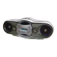
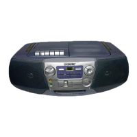
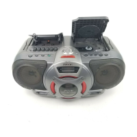
CFD-F10/F10L
Pin No. Pin Name I/O Pin Description
75 X2 O Main system oscillation output (4.19 MHz)
76 RST I System reset input
77 V-CLK O Volume clock output
78 V-DATA O Volume data output
79 SCL O EEPROM clock output
80 SDA I/O EEPROM input/output
 Loading...