– 31 – – 32 –
6-9. SCHEMATIC DIAGRAM — PRE SECTION — • Refer to page 48 for IC Block Diagrams.
Note on Schematic Diagram:
• All capacitors are in µF unless otherwise noted. pF: µµF
50 WV or less are not indicated except for electrolytics
and tantalums.
• All resistors are in Ω and
1
/
4
W or less unless otherwise
specified.
• C : panel designation.
• U : B+ Line.
• Power voltage is dc 9V and fed with regulated dc power
supply from battery terminal.
• Voltage and waveforms are dc with respect to ground
under no-signal (detuned) conditions.
no mark : FM
( ) : PB
< > : REC
[ ] : CD STOP
• Voltages are taken with a VOM (Input impedance 10 MΩ).
Voltage variations may be noted due to normal produc-
tion tolerances.
• Signal path.
F : FM
E : PB
a : REC
J : CD
Note on Printed Wiring Boards:
• X : parts extracted from the component side.
• b : Pattern from the side which enables seeing.
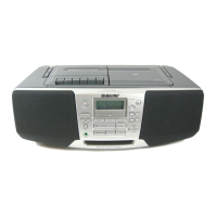
CFD-S22L/S32L
(Page 35)
(Q123) G-11
Q124 G-12
Q221 E-11
Q222 E-11
(Q223) F-11
Q224 G-12
Q301 B-2
Q302 B-3
Q303 B-3
Q501 D-8
Q502 D-8
Q503 E-8
Q504 E-8
Q505 I-8
Q506 E-8
Q507 I-8
(Q509) E-7
Q510 D-9
Q511 D-7
Q512 D-7
Q513 B-9
Q514 C-8
Q951 D-13
Q952 D-13
Q953 D-13
Q955 D-12
Q957 C-13
Q997 B-13
D322 G-11
D323 H-11
D324 B-10
D504 C-8
D505 C-8
(D506) E-7
(D507) E-7
(D508) E-8
D509 E-8
D510 E-8
D511 E-8
D951 D-13
D952 C-13
D953 E-13
D955 C-13
D956 H-11
D957 C-13
IC301 C-3
IC302 E-10
IC304 F-12
IC501 H-9
IC502 H-10
IC503 I-8
IC504 G-7
Q121 E-12
Q122 E-11
• Semiconductor Location
Ref. No. Location Ref. No. Location
( ) : CFD-S32L only
Q301
C
(REC)
• Waveform
1
4Vp-p
19.5µsec
5µsec/div
0.1V/div
w
w
w
.
x
i
a
o
y
u
1
6
3
.
c
o
m
Q
Q
3
7
6
3
1
5
1
5
0
9
9
2
8
9
4
2
9
8
T
E
L
1
3
9
4
2
2
9
6
5
1
3
9
9
2
8
9
4
2
9
8
0
5
1
5
1
3
6
7
3
Q
Q
TEL 13942296513 QQ 376315150 892498299
TEL 13942296513 QQ 376315150 892498299
http://www.xiaoyu163.com
http://www.xiaoyu163.com