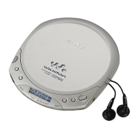
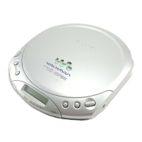
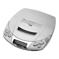
D-E221/E223
1616
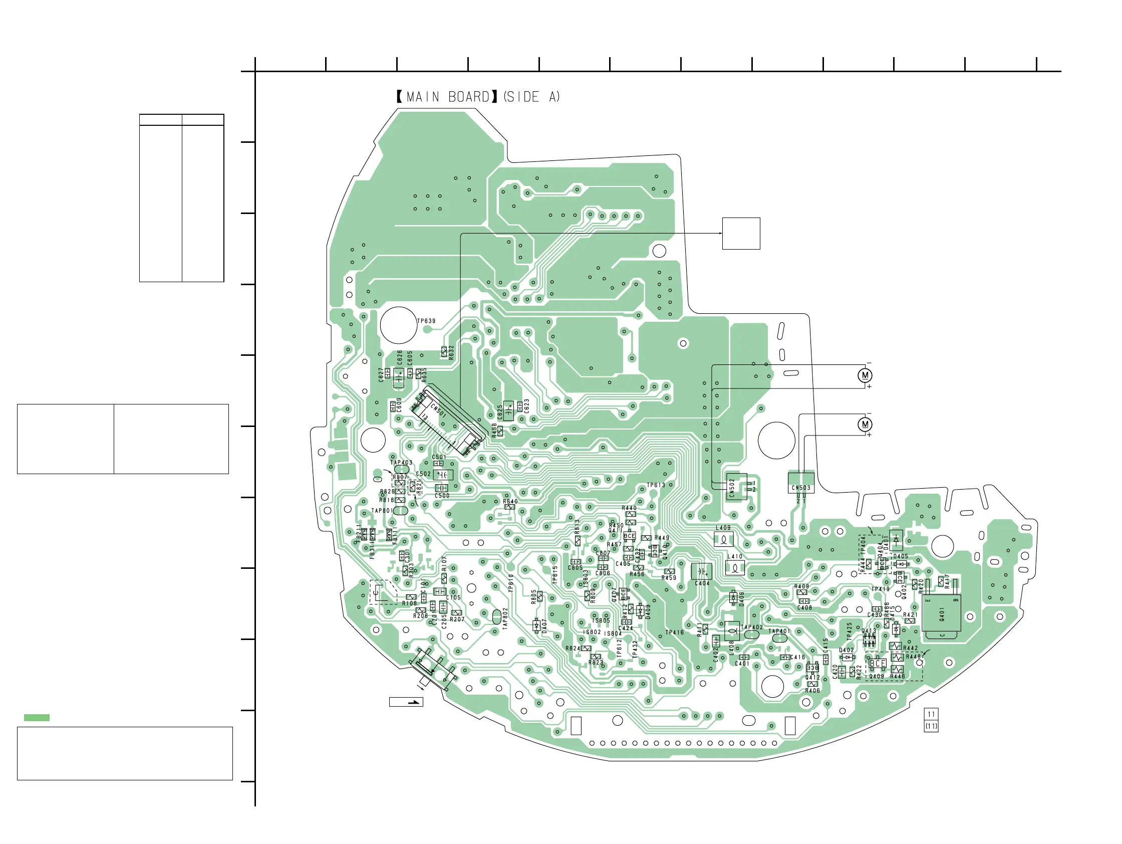
5-5. PRINTED WIRING BOARD — MAIN SECTION —
1
A
B
C
D
E
F
G
H
I
J
234567891011
OPTICAL
PICK-UP
BLOCK
(DAX-23E)
E223
E223
E223
E223:FR MODEL
1-681-329-
RED
BLK
RED
WHT
BLK
BLK
WHT
BLK
M501
SLED
MOTOR
M502
SPINDLE
MOTOR
S803
S803
HOLD
OFF ON
FB601
EXCEPT
US, CND MODEL
Common Note on Printed Wiring Boards:
• X : parts extracted from the component side.
• Y : parts extracted from the conductor side.
•
a
: Through hole.
•
f
: internal component.
• : Pattern from the side which enables seeing.
Common Note on Schematic Diagram:
• All capacitors are in µF unless otherwise noted. pF: µµF
50 WV or less are not indicated except for electrolytics
and tantalums.
• All resistors are in Ω and
1
/
4
W or less unless otherwise
specified.
• % : indicates tolerance.
•
f
: internal component.
• C : panel designation.
• A : B+ Line.
• Power voltage is dc 4.5 V and fed with regulated dc power
supply from external power voltage jack.
• Voltages and waveforms are dc with respect to ground in
playback mode.
no mark : CD PLAY
∗
: Impossible to measure
• Voltages are taken with a VOM (Input impedance 10 MΩ).
Voltage variations may be noted due to normal produc-
tion tolerances.
• Waveforms are taken with a oscilloscope.
Voltage variations may be noted due to normal produc-
tion tolerances.
• Circled numbers refer to waveforms.
• Signal path.
J : CD
• Abbreviation
CND : Canadian model.
FR : France model.
Note:
The components identi-
fied by mark 0 or dotted
line with mark 0 are criti-
cal for safety.
Replace only with part
number specified.
Note:
Les composants identifiés par
une marque 0 sont critiques
pour la sécurité.
Ne les remplacer que par une
piéce portant le numéro
spécifié.
Caution:
Pattern face side: Parts on the pattern face side seen from the
(Side B) pattern face are indicated.
Parts face side: Parts on the parts face side seen from the
(Side A) parts face are indicated.
• Semiconductor
Location (Side A)
D401 G-9
D402 I-9
D405 G-9
D406 H-7
D407 H-4
D409 H-6
D415 H-9
Q401 H-10
Q402 H-9
(Q404) G-9
Q407 H-6
(Q409) I-9
Q410 G-6
Q411 G-6
Q412 I-8
Q413 H-9
Ref. No. Location
( ) : D-E223 only
• Abbreviation
CND : Canadian model.
FR : France model.