– 17 – – 18 – – 20 –– 19 –
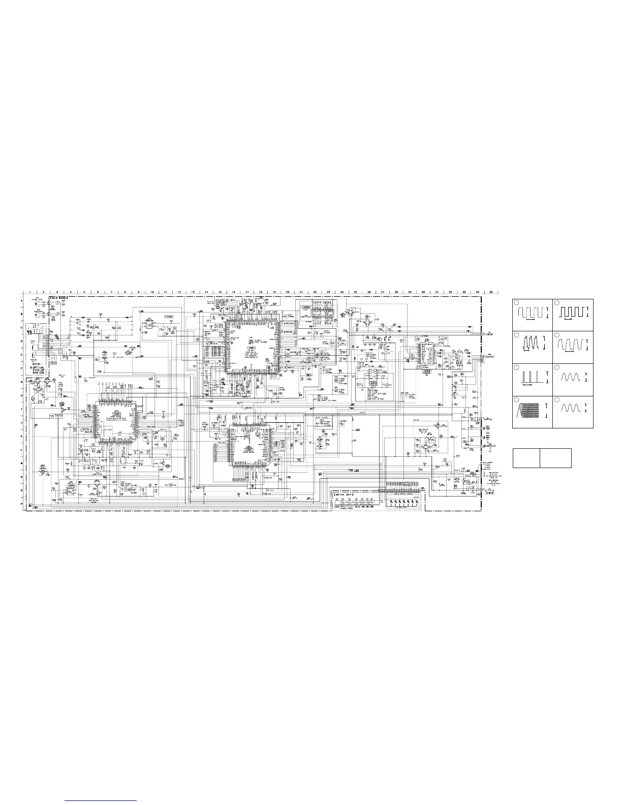
5-4. SCHEMATIC DIAGRAM
D-E660/EJ610/EJ611/EJ613/EJ615/EJ616CK
Note:
• All capacitors are in µF unless otherwise noted. pF: µµF
50 WV or less are not indicated except for electrolytics
and tantalums.
• All resistors are in Ω and
1
/
4
W or less unless otherwise
specified.
Note: Note:
The components identi- Les composants identifiés
fied by mark 0 or dotted par une marque 0 sont cri-
line with mark 0 are cri- tiques pour la sécurité.
tical for safety. Ne les remplacer que par
Replace only with part une piéce portant le
number specified. numéro spécifié.
• U : B+ Line.
• Power voltage is dc 4.5V and fed with regulated dc power
supply from external power voltage jack (J401).
• Voltages and waveforms are dc with respect to ground
under no-signal conditions.
no mark : PLAY
∗
: Impossible to measure
• Voltages are taken with a VOM (Input impedance 10 MΩ).
Voltage variations may be noted due to normal produc-
tion tolerances.
• Waveforms are taken with a oscilloscope.
Voltage variations may be noted due to normal produc-
tion tolerances.
• Circled numbers refer to waveforms.
• Signal path.
J : CD
• Abbreviation
CND : Canadian
AUS : Australian
FR : French
HK : Hong Kong
AR : Argentina
JE : Tourist
G : German
EA : Saudi Arabia
CH : Chinese
EE : East European
C&SA : Central and South America
z
Refer to page 21 – 22 for IC Block Diagrams.
r
Waveforms
1
IC601 wg
CLOCK
5
2 6
3 7
4 8
VOLT/DIV : 0.5 V AC
TIME/DIV : 0.5 µsec
IC601 ih
LRCK
IC601 e;
R4M
IC601 o;
BCK
IC601 rd
MDP
IC601 of
XTAO
IC601 ua
RFAC
IC801 ul
XIN
VOLT/DIV : 0.5 V AC
TIME/DIV : 0.1 µsec
PLAY MODE
VOLT/DIV :0.5 V AC
TIME/DIV : 2 µsec
VOLT/DIV : 0.1 V AC
TIME/DIV : 0.5 msec
VOLT/DIV : 0.5 V AC
TIME/DIV : 5 µsec
VOLT/DIV : 0.5 V AC
TIME/DIV : 0.1 µsec
VOLT/DIV : 0.2 V AC
TIME/DIV : 20 nsec
VOLT/DIV : 0.5 V AC
TIME/DIV : 0.1 µsec
2.1 Vp-p
1.9
µ
sec
1.76 Vp-