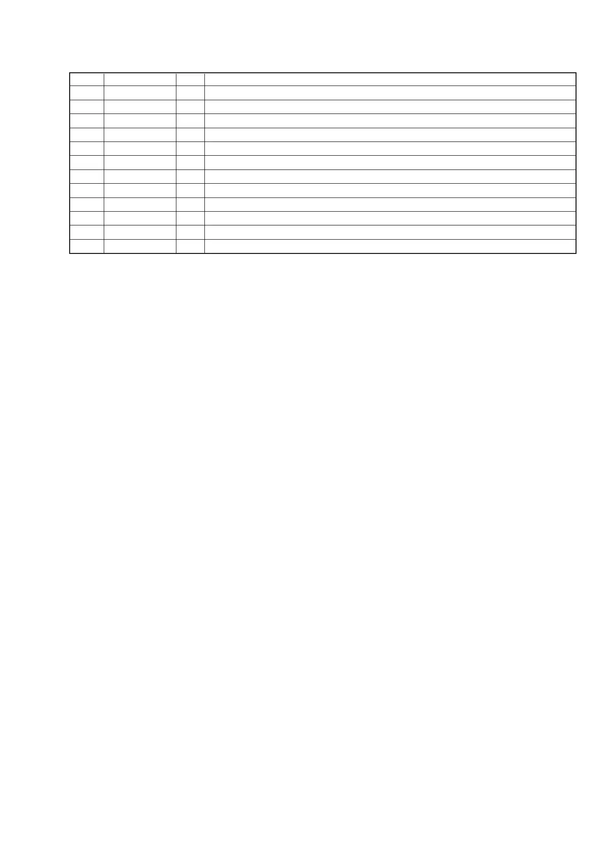
21
D-EJ1000
Pin No.
105
106
107
108
109
110
111
112
113 to 116
117
118
119 to 120
I/O
—
O
I
O
I
O
I
—
O
O
O
O
Pin Name
VDD2
LRCKO
LRCKI
PCMDO
PCMDI
BCKO
BCKI
DVDD
A3 - A0
A10
A11
A12,A13
Description
Power supply (digital)
D/A interface LR clock output (f=Fs)
D/A interface LR clock input
D/A interface Serial data output
D/A interface Serial data input
D/A interface Bit clock output
D/A interface Bit clock input
Power supply (DRAM interface)
DRAM address bus 3 - 0
DRAM address bus 10
DRAM address bus 11 Not used (open)
Test pin Not used (open)