— 40 —
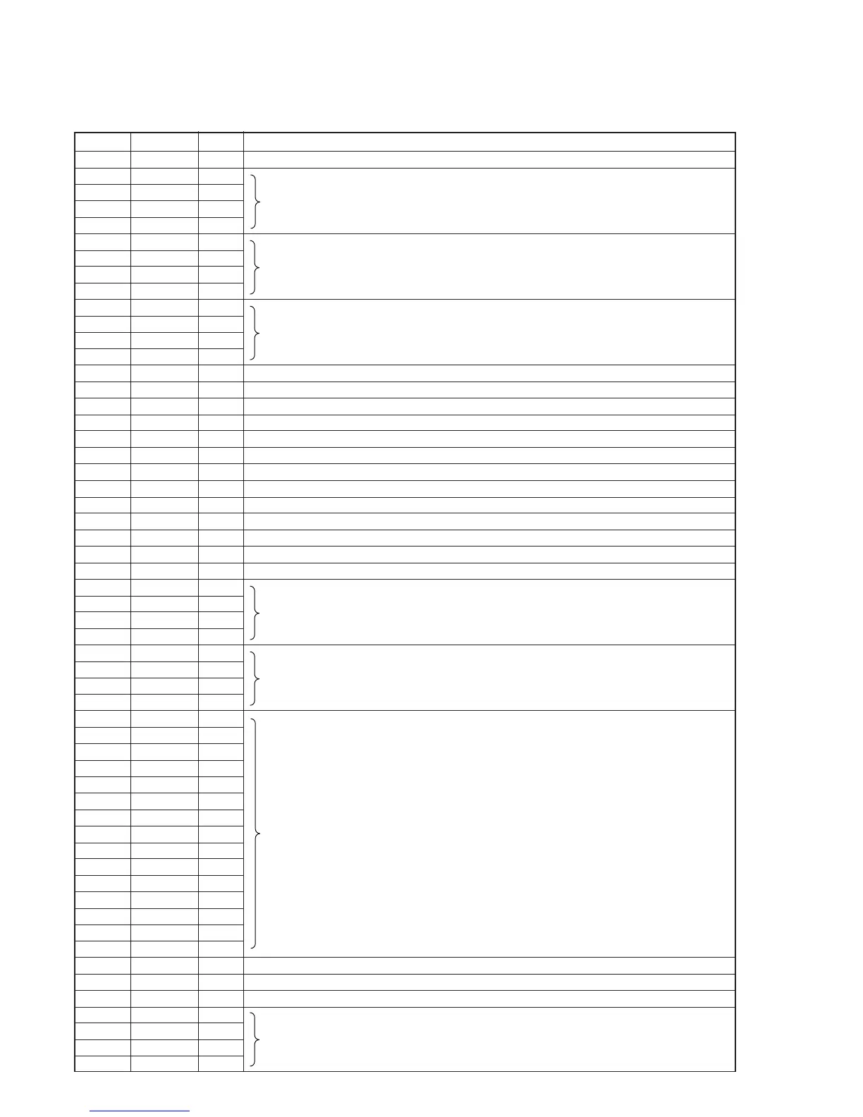
Pin No.
1
2
3
4
5
6
7
8
9
10
11
12
13
14
15
16
17
18
19
20
21
22
23
24
25
26
27
28
29
30
31
32
33
34
35
36
37
38
39
40
41
42
43
44
45
46
47
48
49
50
51
52
53
54
55
56
I/O
O
O
O
O
O
O
O
O
O
I
I
I
I
I/O
I/O
I/O
I/O
–
O
I
I
–
–
–
I
–
–
–
–
–
O
O
O
O
O
O
O
O
O
O
O
O
O
O
O
O
O
O
O
I
I
O
I/O
I/O
I/O
I/O
Function
1-bit general purpose output port. Serial data output.
4-bit general purpose output port.
4-bit general purpose output port.
4-bit general purpose input port Analog input pins for the A/D converter.
2-bit general purpose input/output port.
2-bit general purpose input/output port.
2-bit general purpose input/output ports and for the frequency counter.
2-bit general purpose input/output ports and for the frequency counter.
Ground
Output from the charge pump of the PLL frequency synthesizer.
MF and HF input.
VHF input.
Regulator output pin for PLL.
Common power supply pin (1.8 V to 3.6 V).
External crystal oscillator for system clock oscillation is connected to this pin (75 kHz.)
External crystal oscillator for system clock oscillation is connected to this pin (75 kHz.)
Regulator output pin for oscillator.
Power supply pins for LCD drive.
Common signal of the LCD controller/driver.
These pins are the LCD segment output.
Device selection and reset signal input.
External interrupt signal input.
Beep output pin.
Commonly used pins for 4-bit general purpose input/output ports and for serial interface input.
Pin Name
P1C0/S00
P0A0
P0A1
P0A2
P0A3
P1B0
P1B1
P1B2
P1B3
P1A0
P1A1
P1A2/AD0
P1A3/AD1
P0C0
P0C1
P0D2
P0D3
GND
EO
VCOL
VCOH
VREGO
VDD
XO
XI
VREG1
VLCD0
CAP0
CAP1
VLCD1
COM0
COM1
COM2
COM3
LCD0
LCD1
LCD2
LCD3
LCD4
LCD5
LCD6
LCD7
LCD8
LCD9
LCD10
LCD11
LCD12
LCD13
LCD14
CE
INT
BEEP
P0B0
POB1
P0B2/SCK
P0B3/SI/SO1
• TUNER BOARD IC5 µPD17073
 Loading...