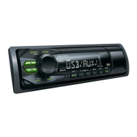
DSX-A50BT
30
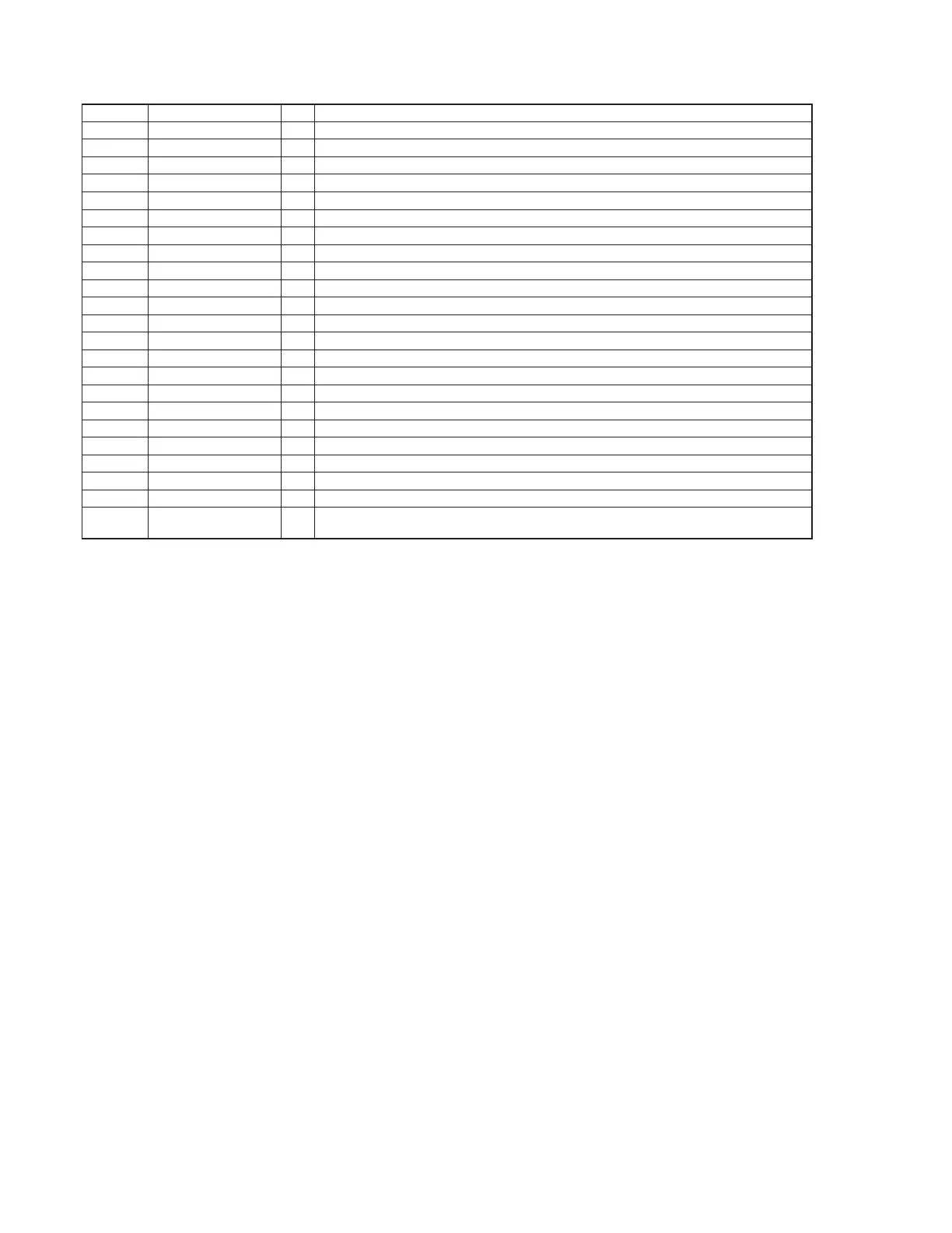
Pin No. Pin Name I/O Description
77 AFILT O Charge pump output terminal (for audio PLL)
78 VVDD2 - Power supply terminal (+3.3V) (for audio PLL)
79 VVDD3 - Power supply terminal (+3.3V) (for system PLL)
80 DVDD - Power supply terminal (+3.3V) (for digital system)
81 DVSS - Ground terminal (for digital system)
82 CP_SCL O Serial data transfer clock signal output terminal Fixed at “H” in this unit
83 SP_SDA I/O Two-way serial data bus terminal Fixed at “H” in this unit
84, 85 GP07, GP06 I/O Not used
86 CP_RESET O Reset signal output terminal Not used
87 TEST0 I Test mode setting terminal Fixed at “L”
88 DVDD - Power supply terminal (+3.3V) (for digital system)
89 DVSS - Ground terminal (for digital system)
90 DVDD15 - External capacitor connection terminal for internal regulator
91 JTRSTB I Reset signal input terminal (for JTAG) Normally: fi xed at “L”
92 JTCK I Clock signal input terminal (for JTAG) Normally: fi xed at “L”
93 JTDI I Data input terminal (for JTAG) Normally: fi xed at “L”
94 JTMS I Mode selection signal input terminal (for JTAG) Normally: fi xed at “H”
95 JTDO O Data output terminal (for JTAG) Normally: open
96 JTRTCK O Return clock signal output terminal (for JTAG) Normally: open
97 TEST1 I Test mode setting terminal Fixed at “L”
98 AVDD1 - Power supply terminal (+3.3V) (for A/D converter)
99 AVSS1 - Ground terminal (for A/D converter)
100 LRREF -
External capacitor connection terminal for audio D/A converter and electrical volume reference
voltage
 Loading...