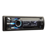
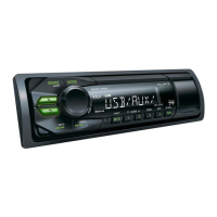
DSX-A50BT
29
MAIN BOARD IC201 LC786800E-00US-H
(USB CONTROLLER, INPUT SELECTOR, AUDIO DSP, ELECTRICAL VOLUME)
Pin No. Pin Name I/O Description
1 LFOUT O Audio signal (front L-ch) output terminal
2 LROUT O Audio signal (rear L-ch) output terminal
3 LVRIN I Audio signal (L-ch) input terminal
4 DACOUT_L O Audio signal (L-ch) output terminal
5 DACOUT_R O Audio signal (R-ch) output terminal
6 RVRIN I Audio signal (R-ch) input terminal
7 RROUT O Audio signal (rear R-ch) output terminal
8 RFOUT O Audio signal (front R-ch) output terminal
9 L1_IN I Audio signal (tuner L-ch) input terminal
10 R1_IN I Audio signal (tuner R-ch) input terminal
11 L2_IN I Audio signal (Bluetooth L-ch) input terminal
12 R2_IN I Audio signal (Bluetooth R-ch) input terminal
13 L3_IN_P I Audio signal (AUX L-ch) input terminal (positive)
14 L3_IN_N I Audio signal (AUX L-ch) input terminal (negative)
15 R3_IN_P I Audio signal (AUX R-ch) input terminal (positive)
16 R3_IN_N I Audio signal (AUX R-ch) input terminal (negative)
17, 18 ATEST01, ATEST02 - Analog test terminal Not used
19 VREFOUT O External reference voltage output terminal
20 VREF_ADC - External capacitor connection terminal for audio A/D converter reference voltage
21 AVSS2 - Ground terminal (for A/D converter)
22 AVDD2 - Power supply terminal (+3.3V) (for A/D converter)
23 to 26 NC - Not used
27 to 30 GP50 to GP53 I/O Not used
31 DVDD - Power supply terminal (+3.3V) (for digital system)
32 DVSS - Ground terminal (for digital system)
33 to 40 GP30 to GP37 I/O Not used
41 DVDD - Power supply terminal (+3.3V) (for digital system)
42 DVSS - Ground terminal (for digital system)
43 REG1_EXTR - Internal regulator reserve terminal
44 DVDD15 - External capacitor connection terminal for internal regulator
45 TXD1 O Serial data output terminal Not used
46 RXD1 I Serial data input terminal Not used
47, 48
OSC_CTL12,
OSC_CTL13
I Clock control signal input terminal Not used
49 DVDD - Power supply terminal (+3.3V) (for digital system)
50 DVSS - Ground terminal (for digital system)
51 RESETB
I Reset signal input from the system controller “L”: reset
52 SIFCK I Serial data transfer clock signal input from the system controller
53 SIFDI I Serial data input from the system controller
54 SIFDO O Serial data output to the system controller
55 SIFCE I Chip enable signal input from the system controller
56 BUSYB O Busy signal output to the system controller
57 USB_IN O USB device detection signal output to the system controller
58, 59 GP40, GP41 I/O Not used
60 WDT_MON O Watch-dog timer status monitor output to the system controller
61 CMD_ERR O Command error signal output to the system controller
62 to 65 GP44 to GP47 I/O Not used
66 DVDD - Power supply terminal (+3.3V) (for digital system)
67 DVSS - Ground terminal (for digital system)
68 UDM1 I/O Two-way USB data (–) bus terminal
69 UDP1 I/O Two-way USB data (+) bus terminal
70 DVSS - Ground terminal (for digital system)
71 UDM2 I/O Two-way USB data (–) bus terminal Fixed at “L” in this unit
72 UDP2 I/O Two-way USB data (+) bus terminal Fixed at “L” in this unit
73 XVDD - Power supply terminal (+3.3V) (for oscillation circuit)
74 X12IN I System clock input terminal (12 MHz)
75 X12OUT O System clock output terminal (12 MHz)
76 DVSS - Ground terminal (for oscillation circuit)
 Loading...