EasyManua.ls Logo

Sony HCD-ZX9 User Manual

Sony HCD-ZX9
94 pages
To Next Page IconTo Next Page
Page #1 background imageLoading...
Page #1 background image
1
Ver. 1.2 2007.02
Model Name Using Similar Mechanism HCD-ZX6/ZX8
CD CD Mechanism Type CDM79B-F1BD81
Section Base Unit Name BU-F1BD81A
Optical Pick-up Name KSM-215DCP/C2NP
TAPE Model Name Using Similar Machanism HCD-ZX6/ZX8
Section Tape Mechanism Type CWM43RR35
SERVICE MANUAL
US Model
Mexican Model
HCD-ZX9
AUDIO POWER SPECIFICATION (US MODEL)
POWER OUTPUT AND TOTAL HARMONIC
DISTORTION:
With 6-ohm loads, both channels driven, from
120 Hz – 10 kHz; rates 140 watts per channel
minimum RMS power, with no more than 10% total
harmonic distortion from 250 milliwatts to rated
output.
Amplifier section
US models:
The following measured at AC 120 V, 60 Hz
Mexican models:
The following measured at AC 127 V, 60 Hz
DIN power output (rated):
140 × 2 + 140 × 2 watts
(6 ohms at 1 kHz, DIN)
Continuous RMS power output (reference):
180 × 2 + 180 × 2 watts
(6 ohms at 1 kHz, 10% THD)
Inputs
PHONO IN (phono jack):
sensitivity 3 mV,
impedance 47 kOhms
MIC (phone jack): sensitivity 1 mV,
impedance 10 kOhms
SPECIFICATIONS
GAME INPUT AUDIO L/R (phono jacks):
sensitivity 250 mV,
impedance 47 kOhms
GAME INPUT VIDEO (phono jack):
1 Vp-p, 75ohms
VIDEO/MD IN L/R (phono jacks):
sensitivity 250 mV/450 mV,
impedance 47 kOhms
Outputs
PHONES (stereo phone jack):
accepts headphones of
8 ohms or more
VIDEO/MD OUT L/R (phono jacks):
voltage 250 mV,
impedance 1 kOhm
VIDEO OUT (phono jack):
max. output level 1 Vp-p,
load impedance 75 ohms
SPEAKER:
FRONT L/R Use only the supplied
speaker SS-ZX9
SURROUND L/R Use only the supplied
speaker SS-ZX9
– Continued on next page –
COMPONENT Hi-Fi STEREO SYSTEM
HCD-ZX9 is the tuner, deck,
CD and amplifier section in
FST-ZX9, LBT-ZX9.
9-887-372-03
2007B04-1
© 2007.02
Sony Corporation
Home Audio Division
Published by Sony Techno Create Corporation

Table of Contents

Question and Answer IconNeed help?

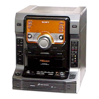
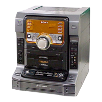
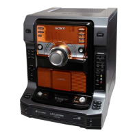
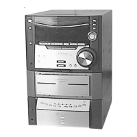
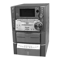
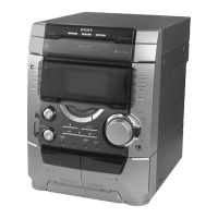
Do you have a question about the Sony HCD-ZX9 and is the answer not in the manual?

Sony HCD-ZX9 Specifications

General IconGeneral
BrandSony
ModelHCD-ZX9
CategoryStereo System
LanguageEnglish

Summary

Service Manual Overview

Specifications Overview

Technical specifications for the system's functions.

Audio Power Specifications

Details on power output and harmonic distortion.

Amplifier Section Specifications

Performance metrics for the amplifier.

Component Specifications

CD/MP3 Player Specifications

Technical details for the CD and MP3 playback functions.

Tape Deck Specifications

Technical details for the tape playback and recording functions.

Tuner Specifications

Technical details for the FM and AM tuner functions.

General System Specifications

Power, dimensions, weight, and supplied accessories.

Critical Service and Safety Notes

Chip Component Handling and Repair

Guidance on replacing chip components and repairing flexible circuits.

Laser Diode Safety Precautions

Warnings and procedures for safe laser diode handling.

US Model Safety Check-out

Procedures for AC leakage tests and safety verification.

Model and Disc Compatibility

Model Identification Details

Identifies US and Mexican model part numbers.

Playable Disc Formats

Lists compatible disc types for playback.

Service Notes and Procedures

CD BU Block Service Position

Location for servicing the CD block assembly.

Tape Mechanism & Panel Board Service Position

Location for servicing tape mechanism and panel board.

Power Board & CD Changer Service Position

Locations for servicing the power board and CD changer.

General System Overview

Button Locations and Reference Pages

Index of buttons and their corresponding page numbers.

Front Panel Controls Diagram

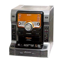
Visual guide to the main unit's buttons and indicators.

Remote Control Functions and Diagram

Guide to remote control buttons and their operations.

Disassembly Instructions

Disassembly Procedure Overview

Flowchart detailing the unit's disassembly sequence.

Case and Loading Panel Disassembly

Steps for removing the unit's case and loading panel.

Front Panel & Tape Mechanism Disassembly

Steps for removing the front panel and tape mechanism.

Game-in/HP, Mic & Back Panel Disassembly

Steps for removing game, mic, and back panel sections.

Component Replacement Procedures

CD Mechanism Section Disassembly

Steps for removing the CD mechanism assembly.

Main Board & Table Assy Disassembly

Steps for removing the main board and table assembly.

SE-130 Board & TD Belt Replacement

Steps for accessing SE-130 board and replacing TD belt.

DC Motor & Optical Pick-up Replacement

Procedures for replacing the DC motor and optical pick-up.

BD81A Board Replacement Procedure

Steps for replacing the BD81A board.

Test Mode Operations

GC Test Mode Details

Procedure for checking indicators, buttons, and software versions.

MC Test Mode Details

Procedure for checking amplifier, tuner, and tape sections.

Tuner Step Change Mode

How to switch AM channel step intervals between 9kHz and 10kHz.

CD Service Mode Procedures

Mode for moving CD sled and cleaning optical pick-up.

Special Operational Modes

CD Repeat Limit Off Mode

Enables CD playback repeat beyond the standard 5-time limit.

CD Ship Mode with Memory Clear

Moves optical pick-up and clears RAM data for shipping or service.

CD Ship Mode without Memory Clear

Moves optical pick-up for vibration durability without clearing RAM.

CD Power Management Mode

Controls power supply to CD BU during tuner function.

Mechanical and Electrical Adjustments

Mechanical Adjustments and Torque

Procedures and specifications for mechanical adjustments and torque.

Electrical Adjustments and Test Modes

Procedures for electrical adjustments and tape deck test modes.

Head Azimuth Adjustment Procedure

Steps for adjusting playback head azimuth for optimal audio output.

CD Section Performance Checks

S-Curve Check Procedure

Verifies the symmetry and level of the CD S-curve waveform.

RF Level Check Procedure

Verifies the clarity and level of the CD RF signal waveform.

Circuit Diagrams Overview

Circuit Board Locations

Visual map showing the placement of internal circuit boards.

Block Diagram: CD Servo Section

Detailed functional block diagram of the CD servo system.

Block Diagram: Tuner/Tape Deck Section

Detailed functional block diagram of the tuner and tape deck.

Block Diagram: Main Section

Detailed functional block diagram of the main processing section.

Diagram Interpretation Guide

Printed Wiring Board & Schematic Notes

Explains symbols and conventions used in diagrams.

Waveform Examples and Interpretation

Illustrates common waveforms and their characteristics.

Printed Wiring Board Layouts

BD Section Wiring Board Layout

Physical layout of the BD section's printed wiring board.

Loading Section Wiring Board Layout

Physical layout of the loading section's printed wiring boards.

Main Section Wiring Board Layout

Physical layout of the main section's printed wiring board.

Power Section Wiring Board Layout

Physical layout of the power section's printed wiring board.

Schematic Diagrams

BD Section Schematic Diagram

Detailed circuit schematic for the BD section.

Loading Section Schematic Diagram

Detailed circuit schematic for the loading section.

Main Section Schematic Diagram (1/4)

Part one of the main section's detailed circuit schematic.

Main Section Schematic Diagram (2/4)

Part two of the main section's detailed circuit schematic.

Main Section Schematic Diagrams

Main Section Schematic Diagram (3/4)

Part three of the main section's detailed circuit schematic.

Main Section Schematic Diagram (4/4)

Part four of the main section's detailed circuit schematic.

Power Section Schematic Diagrams

Power Section Schematic Diagram (1/2)

Part one of the power section's detailed circuit schematic.

Power Section Schematic Diagram (2/2)

Part two of the power section's detailed circuit schematic.

Panel Section Diagrams

Panel Section Wiring Board Layout

Physical layout of the panel section's printed wiring board.

Panel Section Schematic Diagram

Detailed circuit schematic for the panel section.

Volume and Mic Section Diagrams

Volume Section Wiring Board Layout

Physical layout of the volume section's printed wiring board.

Mic Section Wiring Board Layout

Physical layout of the microphone section's printed wiring board.

Volume & Mic Section Schematic Diagram

Detailed circuit schematic for volume and microphone sections.

Switch Section Diagrams

Switch Section Schematic Diagram

Detailed circuit schematic for various switch controls.

Switch Section Wiring Board Layout (1/2)

Physical layout of switch section wiring boards (part 1).

Switch Section Wiring Board Layout (2/2)

Physical layout of switch section wiring boards (part 2).

Jack Section Diagrams

Jack Section Wiring Board Layout

Physical layout of the jack section's printed wiring boards.

Jack Section Schematic Diagram

Detailed circuit schematic for the various jack inputs/outputs.

Lighting Section Diagrams

Lighting Section Wiring Board Layout

Physical layout of the lighting section's printed wiring board.

Lighting Section Schematic Diagram

Detailed circuit schematic for the unit's lighting system.

Surround Section Diagrams

Surround Section Wiring Board Layout

Physical layout of the surround section's printed wiring board.

Surround Section Schematic Diagram

Detailed circuit schematic for the surround sound processing.

Transformer Section Diagrams

Transformer Section Wiring Board Layout

Physical layout of the transformer section's printed wiring board.

Transformer Section Schematic Diagram

Detailed circuit schematic for the power transformer and voltage selector.

Integrated Circuit (IC) Diagrams

IC301 Block Diagram

Functional block diagram of the IC301 chip.

IC251 & IC514/515 Block Diagrams

Functional block diagrams for IC251 and IC514/515 chips.

IC Pin Descriptions

IC101 Pin Descriptions

Detailed pin functions for IC101 (CXD3059AR).

IC101 Pin Descriptions (Continued)

Detailed pin functions for IC101 (CXD3059AR).

IC101 Pin Descriptions (Continued)

Detailed pin functions for IC101 (CXD3059AR).

IC401 Pin Descriptions

Detailed pin functions for IC401 (M3062CMEN).

IC Pin Descriptions (Continued)

IC401 Pin Descriptions (Continued)

Detailed pin functions for IC401 (M3062CMEN).

IC401 Pin Descriptions (Continued)

Detailed pin functions for IC401 (M3062CMEN).

IC901 Pin Descriptions

Detailed pin functions for IC901 (MB90M407PF).

IC901 Pin Descriptions (Continued)

Detailed pin functions for IC901 (MB90M407PF).

Exploded Views and Parts Lists

Back Panel Section Exploded View

Illustrated breakdown of the back panel assembly.

Front Panel Section (1) Exploded View

Illustrated breakdown of the front panel assembly (part 1).

Front Panel Section (2) Exploded View

Illustrated breakdown of the front panel assembly (part 2).

Chassis Section Exploded View

Illustrated breakdown of the main chassis and associated components.

Mechanism Exploded Views

CD Mechanism Section (1) Exploded View

Illustrated breakdown of the CD mechanism assembly (part 1).

CD Mechanism Section (2) Exploded View

Illustrated breakdown of the CD mechanism assembly (part 2).

Electrical Parts List

BD81A Board Component List

Detailed list of components for the BD81A board.

Main Board Component List (Resistors, Transistors)

List of resistors and transistors on the main board.

Various Boards Parts List (Switches, Diodes)

Component list for switches and diodes on multiple boards.

Main Board Component List (Capacitors, Connectors)

List of capacitors and connectors on the main board.

Main Board Component Listings

Main Board Component List (Capacitors, Diodes)

List of capacitors and diodes on the main board.

Main Board Component List (ICs, Jacks, Coils)

List of ICs, jacks, and coils on the main board.

Main Board Component List (Transistors, Resistors)

List of transistors and resistors on the main board.

Main Board Component List (Resistors)

List of resistors on the main board.

Component Listings for Various Boards

Various Boards Parts List (Resistors, Transformers)

Component list for resistors and transformers on various boards.

Mic & Panel Board Parts List (Capacitors, Jacks)

Component list for capacitors and jacks on mic and panel boards.

Panel & Power Board Parts List (Switches, Diodes)

Component list for switches and diodes on panel and power boards.

Power Board Parts List (Capacitors, Transistors)

List of capacitors and transistors on the power board.

Component Listings Across Multiple Boards

Various Boards Parts List (Resistors, ICs, Connectors)

Component list for resistors, ICs, and connectors on various boards.

Surround & TC-A Board Parts List (Capacitors, Transistors)

Component list for capacitors and transistors on surround and TC-A boards.

Various Boards Parts List (Resistors, Switches, Diodes)

Component list for resistors, switches, and diodes on various boards.

Voltage Selector Board Parts List (Resistors, Switches)

Component list for resistors and switches on the voltage selector board.

Miscellaneous Parts List

Miscellaneous Components

List of miscellaneous parts like fuses, wires, and fans.

Revision History

Document Revision Log

Records changes and versions of the service manual.

Related product manuals