ICF-C795RC
– 12 –
– 13 –
– 14 –
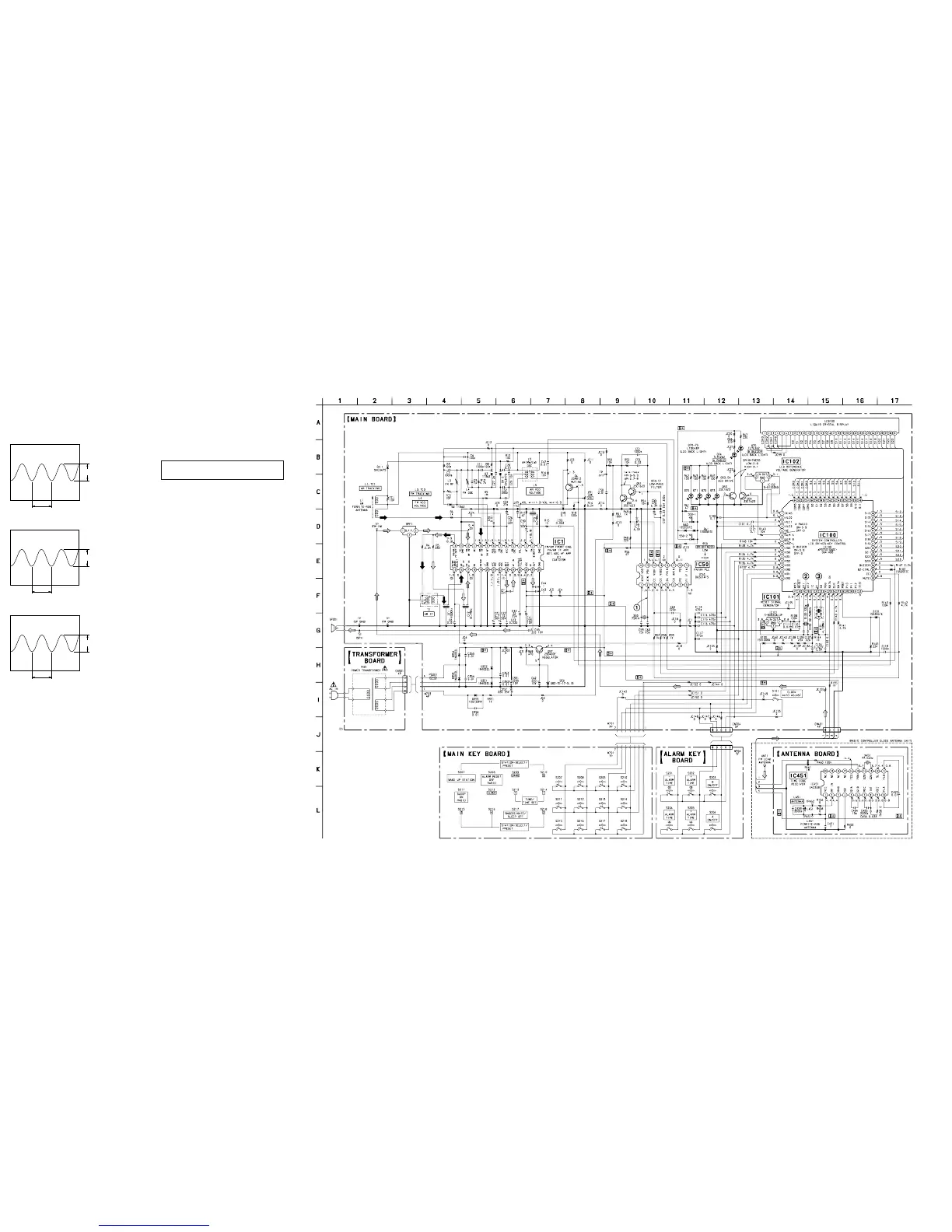
4-2. SCHEMATIC DIAGRAM • See page 17 for IC Block Diagrams.
• Waveforms
– MAIN board –
1 IC50 2 (XIN)
500 mV/DIV, 5 µs/DIV
3 IC100 ws (X1) (*1)
1 V/DIV, 100 ns/DIV
2 IC100 ql (XT1)
1 V/DIV, 10 µs/DIV
*1)
Oscillation will be given out for 250 ms with following conditions.
• Turn the radio on.
• Change the band.
• Change the tuning (manual or preset).
1.8 Vp-p
13.3
µ
s
2 Vp-p
30.5
µ
s
240 ns
2.7 Vp-p
Note on Schematic Diagram:
• All capacitors are in µF unless otherwise noted. pF: µµF
50 WV or less are not indicated except for electrolytics
and tantalums.
• All resistors are in Ω and
1
/
4
W or less unless otherwise
specified.
•
f
: internal component.
• C : panel designation.
• U : B+ Line.
• H : adjustment for repair.
• Voltages and waveforms are dc with respect to ground
under no-signal (detuned) conditions.
no mark : FM
(): AM
• Voltages are taken with a VOM (Input impedance 10 MΩ).
Voltage variations may be noted due to normal produc-
tion tolerances.
• Waveforms are taken with a oscilloscope.
Voltage variations may be noted due to normal produc-
tion tolerances.
• Circled numbers refer to waveforms.
• Signal path.
F : FM
f : AM
Note: The components identified by mark 0 or dotted line
with mark 0 are critical for safety.
Replace only with part number specified.