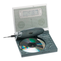
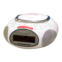
ICF-CD2000/CD2000S
– 45 –
– 46 –
– 47 –
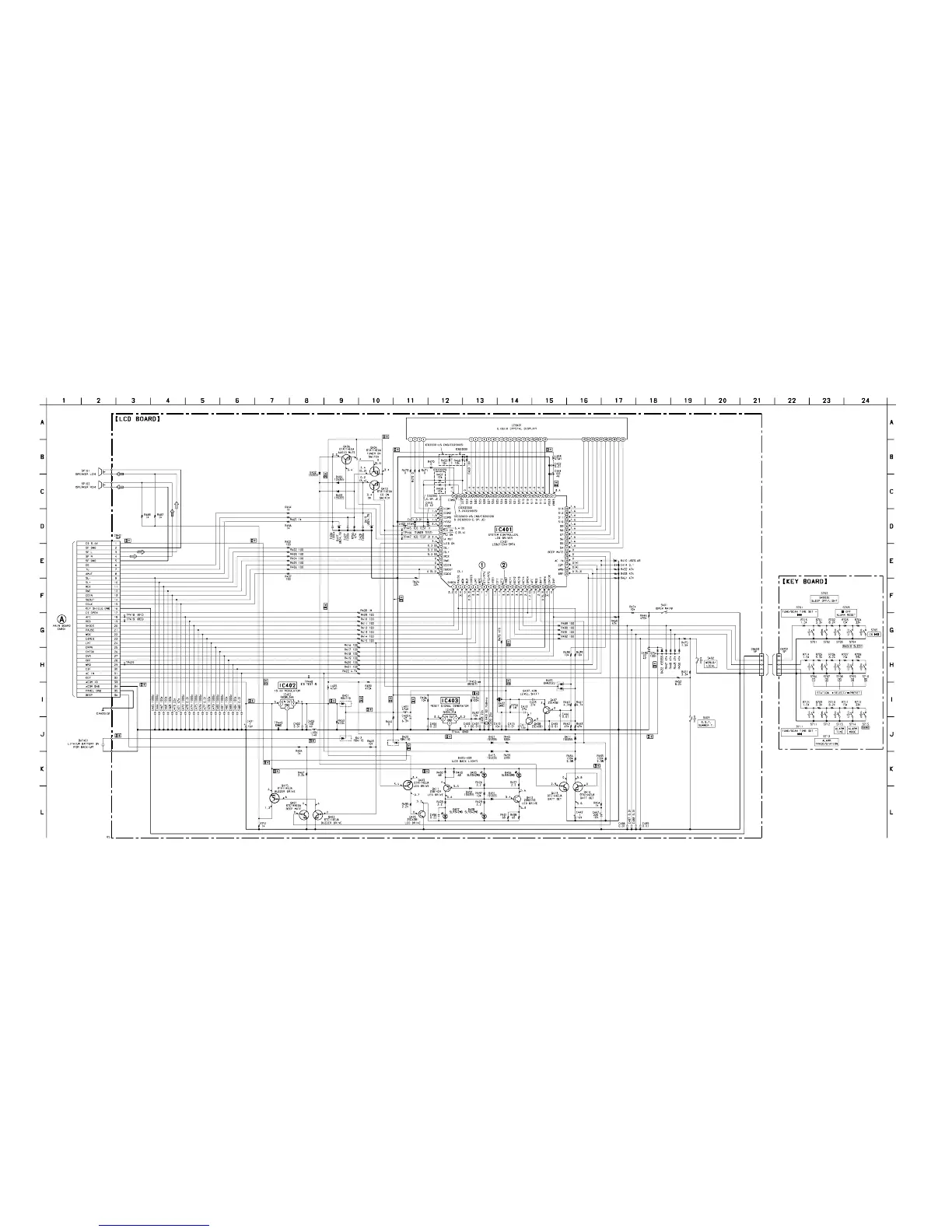
6-7. SCHEMATIC DIAGRAM – LCD/KEY Boards – • See page 42 for Waveforms.
Note on Schematic Diagram:
• All capacitors are in µF unless otherwise noted. pF: µµF
50 WV or less are not indicated except for electrolytics
and tantalums.
• All resistors are in Ω and
1
/
4
W or less unless otherwise
specified.
• % : indicates tolerance.
• C : panel designation.
• U : B+ Line.
• Power voltage is dc 6 V and fed with regulated dc power
supply from external power voltage jack.
• Voltages and waveforms are dc with respect to ground
under no-signal (detuned) conditions.
no mark : FM
[ ] : CD PLAY
∗
: Impossible to measure
• Voltages are taken with a VOM (Input impedance 10 MΩ).
Voltage variations may be noted due to normal produc-
tion tolerances.
• Waveforms are taken with a oscilloscope.
Voltage variations may be noted due to normal produc-
tion tolerances.
• Circled numbers refer to waveforms.
• Signal path.
F : FM
• Abbreviation
CND : Canadian model
JE : Tourist model
SP : Singapore model
(Page 36)