– 29 –
5-3. IC PIN FUNCTION DESCRIPTION
• MAIN BOARD IC401 µPD75304BGF-054-3B9 (SYSTEM CONTROLLER/LCD DRIVER)
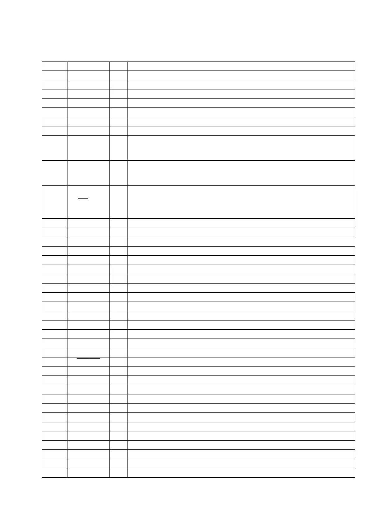
Pin No. Pin Name I/O Function
1 to 3 S12 to S14 O
Segment drive signal output to the liquid crystal display (LCD901)
4 to 6 SEG17 to SEG15 O
Segment drive signal output to the liquid crystal display (LCD901)
7 to 20 SEG14 to SEG1 O
Segment drive signal output terminal Not used (open)
21, 22 COM0, COM1 O
Common drive signal output to the liquid crystal display (LCD901)
23, 24 COM2, COM3 O
Common drive signal output terminal Not used (open)
25 BIAS O
Liquid crystal display drive bias control output terminal
26 to 28 VLC0 to VLC2 —
Terminal for doubler circuit capacitor connection to develop liquid crystal display drive voltage
29 POWER ON I/O
30 CD ON I/O
31 12H/24H I
32 TRACKING
I Setting terminal for the auto tracking adjustment function “L”: auto tracking (fixed at “L”)
33
VSS — Ground terminal
34
ALRAM — Not used (open)
35 BAL B O
Tracking balance adjustment control signal output to the CXA1782BQ (IC501)
36 CLOCK O
Serial data transfer clock signal output to the CXD2508AQ (IC502)
37 XLAT
O Serial data latch pulse signal output to the CXD2508AQ (IC502)
38 AC IN
I AC IN detection signal input terminal (for AC IN check) “H”: AC IN OK
39 SQCK O
Clock signal output for subcode Q data reading to the CXD2508AQ (IC502)
40 P02 O
Not used (open)
41 SQSI
I Subcode Q data input from the CXD2508AQ (IC502)
42 SENS
I Internal status detection signal input from the CXD2508AQ (IC502)
43 C IN I
Track jump count signal input from the CXD2508AQ (IC502)
44 SCOR I
Subcode sync (S0+S1) detection signal input from the CXD2508AQ (IC502)
45 DOOR I
CD lid open/close detect switch (S420) input terminal “L”: open, “H”: close
46 DATA O
Serial data output to the CXD2508AQ (IC502)
47 XRESET
O Reset signal output to the CXA1782BQ (IC501) and CXD2508AQ (IC502) “L”: reset
48
AU MUT O Audio line muting on/off control signal output terminal “L”: muting on
49 BUZZER O
Beep sound output terminal
50 RADIO ON O
Radio system power on/off control signal output terminal “L”: radio on
51 KEY IN1
I Key input terminal WAKE UP TRACK key input (S401)
52 KEY IN2
I Key input terminal ALARM MODE key input (S402)
53 KEY IN3
I Key input terminal ALARM B key input (S403)
54 VDD —
Power supply terminal (+5V)
55 XT1
I Sub system clock input terminal (32 kHz)
56 XT2
O Sub system clock output terminal (32 kHz)
57 NC
— Connected to power supply (+5V)
58 X1
I Main system clock input terminal (4.19 MHz)
59 X2
O Main system clock output terminal (4.19 MHz)
Power on/off control signal output and CD test mode 1 setting terminal
At initial mode: valid/invalid selection of the CD test mode 1 (CD test mode 1 when “L” input)
At normal mode: main power on/off control signal output (power on when “L” output)
Power on/off control signal output and CD test mode 2 setting terminal
At initial mode: valid/invalid selection of the CD test mode 2 (CD test mode 2 when “L” input)
At normal mode: CD power on/off control signal output (power on when “L” output)
Setting terminal for the time display (12/24-hour system) “L”: 12H, “H”: 24H
ICF-CD820; US, Canadian, Australian models and ICF-CD820L; UK model: fixed at “L”,
ICF-CD820; AEP, Italian, Singapore models and ICF-CD820L; AEP, French models: fixed at
“H”
 Loading...