KE-42TS2E(AEP/UK) 3-6
Note:
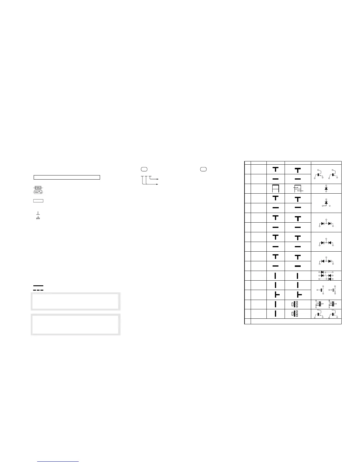
• All capacitors are in µF unless otherwise noted. (pF: µµF)
Capacitors without voltage indication are all 50 V.
• Indication of resistance, which does not have one for rating electrical
power, is as follows.
Pitch: 5 mm
Rating electrical power 1/4 W (CHIP : 1/10 W)
• All resistors are in ohms.
• : nonflammable resistor.
• : fusible resistor.
•
T : internal component.
• : panel designation, and adjustment for repair.
• All variable and adjustable resistors have characteristic curve B, unless
otherwise noted.
• : earth-ground.
• : earth-chassis.
• The components identified by
[ in this basic schematic diagram have
been carefully factory-selected for each set in order to satisfy regulations
regarding X-ray radiation.
Should replacement be required, replace only with the value originally
used.
• When replacing components identified by
], make the necessary
adjustments indicated. (See page 2-1)
• When replacing the part in below table, be sure to perform the related
adjustment.
• All voltages are in V.
• Readings are taken with a 10 M digital multimeter.
• Readings are taken with a color-bar signal input.
• Voltage variations may be noted due to normal production tolerances.
•
*
: Can not be measured.
• Circled numbers are waveform references.
• : B + bus.
• : B – bus.
Note: The components identified by shading and
mark ! are critical for safety. Replace only
with part number specified.
Note: Les composants identifiés par un tramé et
une marque ! sont critiques pour la
sécurité. Ne les remplacer que par une pièce
portant le numéro spécifié.
3-3. SCHEMATIC DIAGRAMS AND PRINTED WIRING BOARDS
• Divided circuit diagram
One sheet of B and Q boards are circuit diagram is divided into three sheets,
each having the code B-a to B-c. For example, the destination
ab1 on the code B-a sheet is connected to ab1 on the B-b sheet.
a b 1
Ref. No.
Circuit diagram division code