KP-EF41HK/ME/MN/SN, EF48HK/ME/MN/SN,
KP-EF53HK/ME/MN/SN, EF61HK/ME/MN/SN RM-871
KP-EF41HK/ME/MN/SN, EF48HK/ME/MN/SN,
KP-EF53HK/ME/MN/SN, EF61HK/ME/MN/SN RM-871
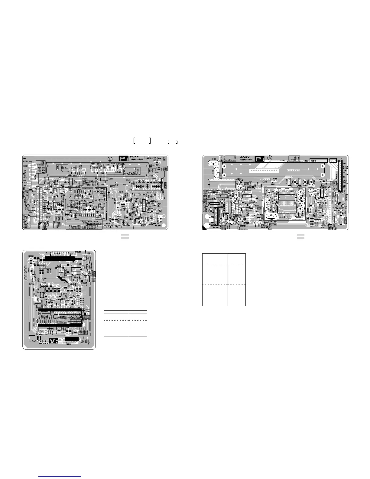
— P1 BOARD (Conductor Side) —
— P1 BOARD (Component Side) —
(p1)
PIP/DVD IN,
PIP TEXT
(v2)
TEXT
– 97 – – 98 –
— V2 BOARD —
• : Pattern from the side which enables seeing.
• : Pattern of the rear side.
V2 BOARD
Terminal name of semiconductors
in silk screen printed circuit (
*
)
*
0
4
1
*
: Refer to Terminal name of
semiconductors in silk screen
printed circuit (see page 63)
Ref.
D3502
D3503
Q3501, Q2502,
Q3506, Q3507,
Q3509, Q3510
P1 BOARD
Terminal name of semiconductors
in silk screen printed circuit (
*
)
*
3
1
2
*
: Refer to Terminal name of
semiconductors in silk screen
printed circuit (see page 63)
Ref.
D2401
Q2301, Q2406,
Q2409, Q2410,
Q2413-Q2418,
Q2427-Q2432,
Q2801, Q2803,
Q2807, Q2809,
Q2810
Q2401-Q2405,
Q2407, Q2408,
Q2411, Q2412,
Q2419-Q2424,
Q2426, Q2802,
Q2804-Q2806,
Q2808
•
: Pattern from the side which enables seeing.
•
: Pattern of the rear side.


 To Next Page