Do you have a question about the Sony MDS-JE510 and is the answer not in the manual?
Technical specifications for system, laser, and disc properties.
Details on input and output connectors and their specifications.
Information on power supply needs and usage patterns.
Critical safety notices regarding laser, general cautions, and component handling.
Guidance for replacing chip components and repairing flexible circuit boards.
Methods for checking AC leakage from exposed metal parts to ground.
Lists part numbers associated with different product countries.
Instructions and details for using the BD board waveform checking jig.
Procedure to reset the system microprocessor when the unit is unresponsive.
How to enter and interpret the retry cause display mode for troubleshooting.
Explanation of symbols and hexadecimal codes shown on the display.
Guide to converting hexadecimal data to binary and mapping to retry causes.
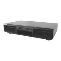
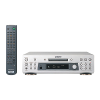
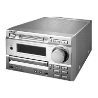
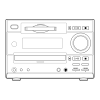
Identification and description of all front panel buttons, knobs, and display elements.
Step-by-step guide for recording audio signals onto a MiniDisc.
Important notes on protecting MDs from erasure and TOC update necessity.
Step-by-step guide for playing audio tracks from a MiniDisc.
Advice on recording, including SCMS, digital input, and track numbering.
How to monitor input signals through the deck's output connectors before recording.
Procedure for recording over previously recorded material on an MD.
Guide to setting optimal recording levels for analog input signals.
How to mark track numbers manually or automatically during recording.
Using prestored audio data to capture the beginning of recordings.
How to perform synchronized recording with external audio equipment.
Steps for dubbing from Sony CD players using synchro-recording.
Using an external timer to schedule MD recording sessions.
How to display total tracks, playing time, remaining time, and disc titles.
Methods to quickly find tracks using AMS, number buttons, or M.SCAN.
Techniques for finding specific points in a track during playback or pause.
How to use repeat functions for tracks, current track, or specific A-B sections.
Setting up and playing tracks in a random, shuffled order.
How to specify playback order and create custom track programs.
Utilizing Auto Space and Auto Pause for efficient MD to tape recording.
Instructions for scheduling MD playback using the timer function.
Important considerations and warnings before performing MD edits.
Procedures for erasing single tracks, all tracks, or portions of tracks.
How to split existing tracks into multiple segments for easier access.
Procedure for merging two adjacent tracks into a single track.
How to change the order of tracks on a recorded MiniDisc.
Guide to creating titles for the MD disc and individual tracks.
Using the remote control to input titles for tracks and the MD.
Procedures for modifying or deleting previously entered titles.
How to cancel the most recent editing operation performed on the MD.
Step-by-step guide for removing the outer case and front panel assembly.
Instructions for removing specific internal mounting brackets.
Steps for detaching and removing the BD (Base Disc) board.
Instructions for disassembling and removing the sub chassis.
Procedure for removing the shutter mechanism components.
Steps for disassembling and removing the over write head assembly.
Instructions for removing the complete slider assembly.
Safety and operational guidelines before entering or using test modes.
Procedures for entering and exiting the unit's test mode.
Explanation of AMS knob, YES, and NO buttons within the test mode interface.
List of available test modes and how to select them via the AMS knob.
Details on entering and using the continuous playback mode.
Details on entering and using the continuous recording mode.
Description of the non-volatile memory mode, noting its non-servicing purpose.
Explanation of button actions relevant to test mode operations.
Details on how to read various displays within the test mode.
Explanation of different display lights and states (e.g., blinking).
Essential safety warnings for checking laser diode emissions.
Guidelines for safely handling the optical pick-up module, noting static sensitivity.
Critical preparatory steps and precautions before performing electrical adjustments.
Instructions for preparing a special disc used for focus bias and error rate checks.
Procedure to adjust the temperature compensation offset for accurate operation.
Detailed steps for setting the laser power output to specified levels.
Step-by-step guide for adjusting the optical pick-up's traverse mechanism.
Detailed procedure for adjusting the focus bias for optimal performance.
Methods for performing error rate checks on CD and MO discs.
How to verify the focus bias after adjustment using specific checks.
Identification of key points for adjustments and connections on the BD board.
Diagram showing the physical layout of the various circuit boards in the unit.
Detailed block diagram illustrating signal paths and functions within the BD section.
Detailed block diagram illustrating signal paths and functions within the main section.
Component placement diagram for the BD board, Side A.
Component placement diagram for the BD board, Side B.
Comprehensive circuit diagram for the BD section of the unit.
Comprehensive circuit diagram for the main section of the unit.
Component layout diagram for the main board, specific to AEP, UK, German models.
Component layout diagram for the main board, excluding AEP, UK, German models.
Component layout diagram for panel sections, specific to AEP, UK, German models.
Component layout diagram for panel sections, excluding AEP, UK, German models.
Detailed circuit diagram for the panel section, covering display, control, and other boards.
Internal functional block diagram for IC101.
Internal functional block diagram for IC121.
Internal functional block diagram for IC121.
Internal functional block diagram for IC152.
Internal functional block diagram for IC171.
Internal functional block diagram for IC192.
Internal functional block diagram for IC301.
Internal functional block diagram for IC307.
Internal functional block diagram for IC308.
Internal functional block diagram for IC309.
Internal functional block diagram for IC310.
Internal functional block diagram for IC311.
Internal functional block diagram for IC315.
Detailed pin list and function descriptions for IC101.
Pin assignments and functions for IC121 (CXD2650R/CXD2652AR).
Further pin assignments and functions for IC121.
Remaining pin assignments and functions for IC121.
Pin assignments and functions for IC307.
Further pin assignments and functions for IC307.
Pin assignments and functions for IC316 System Control.
Further pin assignments and functions for IC316.
Remaining pin assignments and functions for IC316.
Diagram showing the breakdown of the main unit assembly.
Diagram illustrating the assembly of the front panel components.
Diagram showing the disassembly of the first part of the mechanism deck.
Diagram showing the disassembly of the second part of the mechanism deck.
List of capacitors and diodes used in the BD section.
List of integrated circuits used in the BD section.
List of inductors and transistors used in the BD section.
List of resistors used in the BD section.
List of parts for the Control (SW) board, including switches and connectors.
List of parts for the display board, including capacitors and indicators.
List of transistors and resistors for the Main section.
List of switches and connectors for the SW section.
Detailed list of capacitors used in the Main section.
List of connectors, diodes, and ICs for the Main section.
List of resistors and transistors for the Main section.
List of resistors for the Main and SW sections.
List of switches, transformers, and vibrators for Main/SW sections.
Listing of miscellaneous items like cords, adapters, and indicators.
List of included accessories such as remote, manuals, and battery covers.
List of screws and fasteners used in the unit's assembly.
| Brand | Sony |
|---|---|
| Model | MDS-JE510 |
| Category | Stereo System |
| Language | English |