Do you have a question about the Sony HCD-MD313 and is the answer not in the manual?
Specifications for the CD mechanism, base unit, and optical pick-up.
Specifications for the MD mechanism and optical pick-up.
Continuous and music power ratings for different models and regions.
Details on input/output jacks and speaker impedance requirements.
Details on FM and AM tuning ranges and intermediate frequency.
Power requirements, consumption, dimensions, and mass.
Explains the system's malfunction display and error codes.
Details on identifying different models and their corresponding parts numbers.
Guidelines for safely handling the optical pick-up block.
Instructions for safely checking the laser diode emission.
Precautions for replacing chip components, especially tantalum capacitors.
Guidelines for soldering and repairing flexible circuit boards.
Identifies critical safety components and replacement procedures.
Step-by-step instructions for removing the disc table when the power is off.
Procedure to verify the functionality of the fluorescent indicator tube, buttons, and LEDs.
Steps to check the sub clock signal using an oscilloscope.
Method for checking audio-related functions and displays in TA mode.
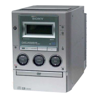
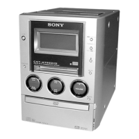
Identifies and describes the buttons and jacks on the front panel.
Identifies and describes the terminals and connectors on the rear panel.
Lists and describes all buttons on the remote controller for various functions.
Step-by-step guide to set the system's clock time accurately.
Instructions on how to modify pre-set timer times.
Instructions for disassembling the outer case of the unit.
Steps to separate the front panel from the MD mechanism deck.
Procedures for removing the back panel and associated jack board.
Steps to disassemble the MD mechanism deck unit.
Steps for disassembling the CD mechanism deck.
Instructions for removing the BD (MD) board from the unit.
Procedures for disassembling the disc table assembly.
Instructions for removing and disassembling the sub chassis.
Steps for disassembling the optical pick-up unit.
Instructions for removing the over write head component.
Procedures for removing the slider complete assembly.
Important considerations for installing the slider assembly correctly.
Instructions for disassembling the shutter assembly, including stopper washer and shafts.
Important safety and operational guidelines before entering test mode.
Explains modes related to laser emission and recording operations.
Procedures for entering and exiting the test mode.
Describes how to use the VOLUME knob and buttons within test mode.
Lists the available test modes and how to select them.
Instructions for entering, operating, and ending continuous playback mode.
Steps for entering, operating, and ending continuous recording mode.
Explains the EEP mode and its function for non-volatile memory.
Procedures for accessing and exiting the error history mode.
How to navigate through different memory types for error history.
Guide on viewing recorded error history data.
Describes the specific functions of the REC and Disc Eject buttons in test mode.
Explains various displays shown during test mode operations (Mode, Error Rate, Address, Auto Gain).
Interprets additional display indicators like REC and DISC status.
Safety measures for checking laser diode emission.
Guidelines for handling the optical pick-up to prevent static damage.
Important notes and preparation before performing electrical adjustments.
Procedure for preparing a special disc for adjustment tests.
Steps to adjust the temperature compensation offset.
Procedure for adjusting the laser power output.
Detailed steps for performing the traverse (E-F balance) adjustment.
Procedure for adjusting the focus bias.
Steps to check the CD error rate.
Procedure for checking the MO error rate.
Method to check the focus bias tolerance.
Identifies adjustment and connection points on Side A of the BD (MD) board.
Identifies adjustment and connection points on Side B of the BD (MD) board.
Steps for performing focus bias adjustment on the CD section.
Describes the expected RF signal eye pattern for reference.
Procedures for checking S-curve and RF signal levels.
Method for checking the E-F balance (traverse) in the CD section.
Details the expected traverse waveform and its specifications.
Information regarding the focus/tracking gain adjustment.
Identifies specific locations on the BD (CD) board for adjustments.
Illustrates the physical location of all major circuit boards within the unit.
Illustrates the signal paths and component interactions within the CD section.
Depicts the signal paths and component interactions within the MD section.
Illustrates the signal flow and interconnections within the main section of the system.
Shows the component placement on the front side of the CD board.
Shows the conductor patterns on the back side of the CD board.
Detailed schematic illustrating the electronic components and connections in the CD section.
Component placement diagram for the front side of the MD board.
Conductor pattern diagram for the back side of the MD board.
Schematic details for the first part of the main section.
Schematic details for the second part of the main section.
Schematic details for the third part of the main section.
Component layout for the first part of the main board.
Component layout for the second part of the main board.
Component layout for the third part of the main board.
Component placement diagram for the audio board.
Detailed schematic illustrating the electronic components and connections in the audio section.
Component placement for the panel board.
Component placement for the MD LED board.
Component placement for the jack board.
Component placement for the transformer board.
Component placement for the power amp board.
Circuit diagram for the panel board.
Circuit diagram for the MD LED board.
Circuit diagram for the jack board.
Circuit diagram for the transformer board.
Circuit diagram for the power amp board.
Visual representations of key signals in the CD section for analysis.
Visual representations of key signals in the MD section for analysis.
Visual representations of key signals in the main section.
Visual representations of key signals in the audio section.
Internal block diagram of IC101, detailing its functional units.
Internal block diagram illustrating the functionality of IC102.
Internal block diagram detailing the functional units of IC103.
Internal block diagram for IC104, likely related to MD or audio processing.
Internal block diagram detailing the functional blocks of IC201.
Internal block diagram of IC101, detailing its functional units.
Internal block diagram illustrating the functionality of IC121.
Internal block diagram detailing the functional blocks of IC152.
Internal block diagram for IC570, detailing its functions.
Internal block diagram illustrating the functionality of IC603.
Internal block diagram for IC801, detailing its functions.
Internal block diagram illustrating the functionality of IC1500.
Detailed description of each pin on IC101 for the BD (MD) board.
Detailed description of each pin on IC121 for the BD (MD) board.
Further details on pin functions for IC121 on the BD (MD) board.
Additional pin function details for IC121 on the BD (MD) board.
Detailed description of each pin on IC316 for MD system control.
Further details on pin functions for IC316.
Detailed description of each pin on IC601 for master control.
Further details on pin functions for IC601.
Exploded diagram of the front panel components with part references.
Exploded diagram of the chassis components with part references.
Exploded diagram of the MD mechanism deck (MDM-3D) components.
Exploded diagram of the MD mechanism deck (MDM-3D) components.
Exploded diagram of the CD mechanism deck components.
Exploded diagram of the CD mechanism deck components.
List of electrical components for the audio section, including capacitors, connectors, diodes, and ICs.
List of components for audio and BD (CD) boards, including resistors, transistors, capacitors, and connectors.
List of components for BD (MD) and Jack boards, including resistors, transistors, ICs, and connectors.
List of components for the BD (MD) board, including capacitors, connectors, diodes, ICs, coils, and transistors.
Detailed list of resistors used on the BD (MD) board.
Continuation of component lists for BD (MD) and Jack boards.
List of various capacitors, transistors, and resistors for the system.
List of components for the Main section, including ground terminals, ferrite beads, ICs, transistors, and resistors.
List of components for Main, MD-LED, and Panel boards, including resistors, LEDs, switches, and capacitors.
List of components for the Panel section, including resistors, LEDs, ICs, jacks, switches, and fuses.
List of components for Panel, Power Amp, and ST Terminal sections, including switches, capacitors, transistors, and resistors.
List of components for SW and Transformer sections, including connectors, switches, fuses, and hardware.
| Type | Mini Hi-Fi System |
|---|---|
| Disc Compatibility | CD, MD |
| Tuner | FM/AM |
| Speakers | 2-way speakers |
| MD Player/Recorder | Yes |
| Remote Control | Yes |
| Audio Channels | 2.0 |
| Speakers Count | 2 |
| Power Output | 100W |
| Functions | CD, MD, Radio, Cassette |
| CD Player Type | Single disc |
| Cassette Deck | Double Cassette Deck |