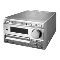
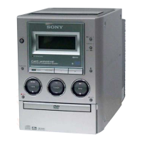
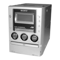
– 78 –
• BD (MD) BOARD IC316 M30610MC-116FP (MD SYSTEM CONTROL)
Pin No. Pin Name I/O Function
1,2 (JOG0, JOG1) I Encoder switch signal input terminal Not used (fixed at “H”)
3,4
DAOUT1, DAOUT2
O Not used (fixed at “L”)
5 SQSY I Subcode Q sync (SCOR) input from the CXD2652AR (IC121)
6 REMCON I Remote control signal input
7 EMP O De-emphasis control signal output to the AK4520 (IC201)
8 BYTE I External data bus line byte select signal input terminal “L”:16bit “H”: 8bit (fixed at “L”)
9 CNVSS I Processor mode select signal input terminal (fixed at “L”)
10 XIN-T I Sub system clock input tarminal Not used (fixed at “L”)
11 (XOUT-T) O Sub sytem clock output tarminal Not used (fixed at “L”)
12 SYSTEM-RST I MD reset signal input from the M62016 (IC603)
13 XOUT O Main system clock signal output terminal
14 GND — Ground terminal
15 XIN I Main sytem clock signal input terminal
16 +3V — Power supply terminal (+3.3V)
17 NMI — Connecting to power supply
18 AMUTE — Not used (fixed at "L")
19 PWR-DWN O Power down detect signal output to the LA5620 (IC570)
20 DQSY I Digital in U-bit CD format subcode Q sync (SCOR) input from theCXD2652SAR (IC121)
21 STB I Stand-by signal input terminal Not used (fixed at “L”)
22 DA-RST I D/A converter reset signal input terminal Not used (fixed at “L”)
23 XINT I Interrupt status input from the CXD2652AR (IC121)
24 DA-EN O D/A converter enable signal output to the AK4520 (IC201)
25 AD-EN O A/D converter enable signal output to the AK4520 (IC201)
26 MEC-BUSY O Mecha-busy signal output to the master control (IC601)
27 FLCS O Display clear signal output terminal Not used (fixed at “L”)
28 FLCLK O Display data clock signal output terminal Not used (fixed at “L”)
29 — Not used (fixed at “L”)
30 FLDATA O Display data signal output terminal Not used (fixed at “L”)
31 TXD O MD control data signal output to the master control (IC601)
32 RXD I MD control data signal input to the master control (IC601)
33 CLK I MD control data clock signal input to the master control (IC601)
34 MAS-BUSY I Master-busy signal input from the master control (IC601)
35 SWDT O Writing data signal output to the CXD2652AR (IC121)
36 SRDT I Reading data signal input from the CXD2652AR (IC121)
37 SCLK O Serial clock signal output to the CXD2652AR (IC121)
38 XLAT O Serial latch signal output to the CXD2652AR (IC121)
39 O Clock signal output terminal Not used (fixed at “L”)
40 DIG-RST O Reset signal output enable signal output to the CXD2652AR (IC121)
41 SENS I Status (SENSE) input from the CXD2652AR (IC121)
42 SCTX O Recording data output enable signal output to the CXD2652AR (IC121)
43 XINT O Not used (fixed at “L”)
44 WRPWR O Laser power selection signal output to the CXD2652AR (IC121)
45 MNT3 I Monitor 3 signal input from the CXD2652AR (IC121)
46 MNT2 I Monitor 2 signal input from the CXD2652AR (IC121)
47 MNT1 I Track jump detection signal input from the CXD2652AR (IC121)
48 MNTO I Focus OK signal input from the CXD2652AR (IC121)
49 LDON O Laser diode ON signal output terminal
w
w
w
.
x
i
a
o
y
u
1
6
3
.
c
o
m
Q
Q
3
7
6
3
1
5
1
5
0
9
9
2
8
9
4
2
9
8
T
E
L
1
3
9
4
2
2
9
6
5
1
3
9
9
2
8
9
4
2
9
8
0
5
1
5
1
3
6
7
3
Q
Q
TEL 13942296513 QQ 376315150 892498299
TEL 13942296513 QQ 376315150 892498299
http://www.xiaoyu163.com
http://www.xiaoyu163.com