Do you have a question about the Sony MHC-V11 and is the answer not in the manual?
Detailed audio output power and distortion characteristics for the unit.
Specifications for the amplifier circuit, including rated power and RMS output.
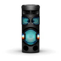
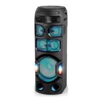
Details about the speaker system, including tweeter and woofer specifications.
Description of input ports, voltage, and impedance requirements.
Description of output ports, voltage, and impedance characteristics.
Technical specifications of the compact disc and digital audio player mechanism.
Details about the USB port type and maximum current capacity.
List of audio formats supported for MP3 discs and USB devices.
Specifications for the FM stereo superheterodyne tuner.
Communication system, range, frequency band, and supported BLUETOOTH profiles.
Unit dimensions, mass, and supplied accessories list.
Precautions for handling the optical pick-up block to prevent electrostatic discharge damage.
Guidelines for safely checking the laser diode emission from the optical pick-up block.
Characteristics and handling guidelines for unleaded solder used in the unit's construction.
Information on whether to replace entire boards or individual components.
Important instruction regarding the simultaneous replacement of BT and NFC boards.
Information on using specific test discs for confirming unit operation and checks.
A flowchart outlining the sequence of disassembly steps for the unit.
Procedure for removing the left and right side covers of the unit.
Detailed steps for removing the top cover assembly from the unit.
Instructions for the removal of the main and microphone volume knobs.
Procedure for disassembling and accessing the main control board.
Steps for removing the top cover assembly and the NFC board.
Detailed procedure for removing the CD loader mechanism (CDM1).
Procedure for disassembling and accessing the Bluetooth (BT) board.
Steps involved in removing the main chassis block of the unit.
Procedure for removing the front panel assembly and its components.
Instructions for disconnecting the wiring harness for the tweeter units.
Procedure for removing the tweeter units (SP2 and SP3).
Steps for removing the LED A and LED B circuit boards.
Procedure for removing the woofer unit (SP1).
Instructions for removing the loader mechanism as a complete block.
Procedure for disassembling and accessing the main circuit board.
Procedure for disassembling and accessing the power supply unit (PSU) board.
Method to display and verify the unit's current software version.
Procedure to reset all MPEG settings and clear the Bluetooth linked list.
Procedure to check the FM auto-stop function using a signal generator.
General notes and preparation for performing electrical checks on the CD section.
Procedure to check the RF signal output using an oscilloscope for eye pattern verification.
Overall system block diagram showing interconnections between major components.
Block diagram illustrating the power supply unit's architecture and voltage distribution.
Component layout and tracing guide for the main circuit board.
Detailed circuit schematic for the main board, part 1 of 9.
Detailed circuit schematic for the main board, part 9 of 9.
Detailed circuit schematic diagram for the power supply board.
Exploded view illustrating the disassembly and parts of the side covers.
Exploded view showing the disassembly and parts of the top cover assembly.
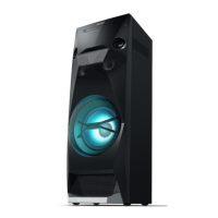
Exploded view detailing the woofer unit and its associated components.
Exploded view illustrating the disassembly and parts of the front panel.
Exploded view of the main internal chassis and major components.
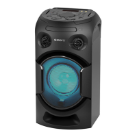
| Speaker Type | 2-way |
|---|---|
| Bluetooth | Yes |
| USB Playback | Yes |
| FM Radio | Yes |
| Karaoke Function | Yes |
| Number of optical discs | 1 |
| Audio formats supported | MP3, WMA |
| RMS rated power | 470W |
| USB port | Yes |
| USB version | 2.0 |
| Near Field Communication (NFC) | Yes |
| Width | 290 mm |
| Height | 600 mm |
| Weight | 10 kg |
| Optical disc player type | CD |
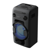
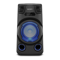
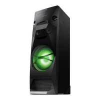
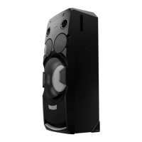
| Type | Home audio mini system |