Do you have a question about the Sony PlayStation SCPH-1002 and is the answer not in the manual?
General specifications for SCPH-9000 models including power, dimensions, and mass.
General specifications for SCPH-9001 model including power, dimensions, and mass.
General specifications for SCPH-9002/A/B/C models including power, dimensions, and mass.
General specifications for SCPH-9003 model including power, dimensions, and mass.
Diagram showing the assembly of the main unit with all components labeled.
Highlights safety-critical parts and warnings regarding hazardous radiation exposure.
Details required test specifications for RF Level, Jitter, PP Level, and Tracking Level.
Important note on wiring the VC Line (CL710) during adjustments.
Explains the units used for capacitors, resistors, and inductors in the manual.
Procedure for dielectric voltage and insulation resistance tests after repair.
Guidelines for checking performance before replacing the optical device.
High-level block diagram of the PU-23 board and its main functional sections.
Detailed schematic illustrating signal paths and connections between ICs on the PU-23 board.
Guidelines for interpreting Printed Wiring Boards and Schematic Diagrams, including safety markings.
Visual layout of the PU-23 board showing component positions and numbering.
Highlights differences in the PU-23 board layout based on model suffix (-11/-21/-31/-41/-51).
Circuit diagram for CPU, DRAM, and Boot ROM sections of the PU-23 board.
Circuit diagram for GPU, Clock Generator, and SGRAM sections of the PU-23 board.
Circuit diagram for power regulation ICs and audio amplifier sections of the PU-23 board.
Circuit diagram for control, RF signal processing, and motor drive sections of the PU-23 board.
Waveform measurements for CPU (IC103) and Boot ROM (IC102) in different operational modes.
Waveform measurements for GPU (IC203) and SGRAM (IC201) signals.
Waveform measurements for Audio (IC732) and Video (IC502) output signals.
Waveform measurements for control (IC304) and RF (IC723) signals.
Schematic diagram of the Power Block (1-468-366-11) with component layout.
Schematic diagram of the Power Block (1-468-365-11) with component layout.
Schematic diagram of the Power Block (1-468-303-13) with component layout.
Schematic diagram of the Power Block (1-468-243-11) with component layout.
Notes on parts, classification by availability, and identification of safety-critical components.
Detailed list of components specific to the PU-23 Board.
List of capacitors from C215 to C728, including part numbers and descriptions.
Parts list for connectors, diodes, and ferrite beads, noting model variations.
List of integrated circuits (ICs) and other parts like resistors and network resistors.
Detailed parts list for resistors, inductors, and transistors.
List of links, switches, and crystal components used in the system.
List of resistors, power cords, adapters, and other accessories.
List of capacitors and filters for the Power Block (9000).
List of diodes, fuses, ICs, and resistors for the Power Block (9000).
List of capacitors and filters for the Power Block (9001).
List of diodes, fuses, ICs, and resistors for the Power Block (9001).
List of capacitors and filters for the Power Block (9002).
List of diodes, fuses, ICs, and resistors for the Power Block (9002).
List of capacitors and filters for the Power Block (9003).
List of diodes, fuses, ICs, and resistors for the Power Block (9003).
List of resistors, transistors, and switches with their respective part numbers.
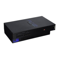
| Model | SCPH-1002 |
|---|---|
| Category | Game Console |
| Manufacturer | Sony |
| RAM | 2 MB |
| VRAM | 1 MB |
| Sound RAM | 512 KB |
| CD-ROM Drive | 2x speed |
| Resolution | 256 × 224 to 640 × 480 |
| Video Output | Composite, S-Video, RGB |
| Audio Output | Stereo |
| Controller Ports | 2 |
| Memory Card Slots | 1 |
| Weight | 1.2 kg |
| Power Supply | Internal |
| Release Year | 1994 |
| Media | CD-ROM |
| CPU | MIPS R3000A 33.8688 MHz |
| Ports | Serial I/O, Parallel I/O |