A
B
C
D
E
F
G
H
J
K
L
M
N
0
p
6-4. GIRCUIT BOARQS
6-5. SCHEMATIC DIAGRAMS
1. 2
4.. 5
6
w
C
F
V (PVM-13420/1343MD ONLY)
QC
OE
BA (PVM-13420/1343MD ONLY)
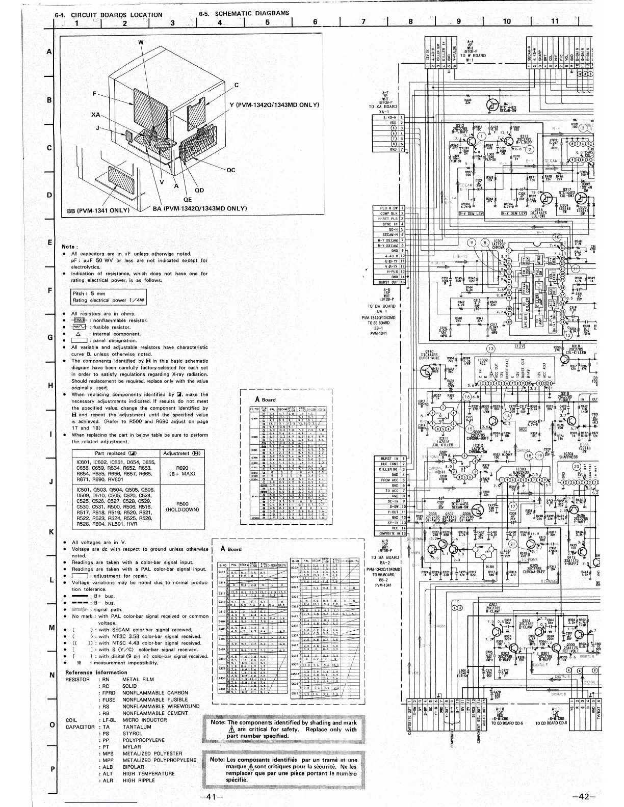
Note:
• All capa<:itors are in µ F unless otherwise noted.
pF : µµ F 50 WV or Jessi are not indicated except for
electrolytics,
•
Indication of resistance, which· doe.s not have one for
rating electrical power, is as follows.
Pitch: 5 mm
Rating electrical power 1 /4W
• All resistors are in ohms.
•
~
: nonflammable resistor.
•
~
: fusible resistor.
•
~
: intemal component.
• C=:=] : panel ·· designation.
• All variable and adjustable resistors have characteristic
curve B, unless . otherwise noted.
• The components ·identified· by 8 in this basic schematic
diagram have been carefully factory-selected for each set
in order to satisfy regulations regarding X-ray radiation.
Should replacement be required, replace only with the value
originally used;
• When replacing components identified .by !.iii. make the
necessary adj.ustments ihdicated. If results do riot meet
the specified value, change the component identified by
8 and repeat the adjustment until the specified value
is achieved. (Refer to. R500 and· R690 · adjust on page
17 and 18)
• When replacing the p.irt in below table be sure to perform
the related adjustment.
Part replaced (!.iii) ..
Adjustment
(8)
IC601, IC602. IC651, D654, D655,
C658, C659, R634, R652, R653, R690
R654, R655, R656, R657, R665, (B+ MAX)
R671, R690, RV601
IC501, 0503 .• Q504, Q505. 0506,
D509, D510, C505, C520. C524,
C525, C526, C527, C528. C529.
R500
C530, C531, R500, R506, R516,
(HOLD-DOWN}
R517, R518, R519, R520, R521,
R522, R523, R524, R525, R526,
R528, R804, NL501, HVR
i----· ---· -·-1
l A Board I
I I
I I
I I
I I
I I
I I
I I
I I
I I
I I
I I
I I
I I
L____ _ _____ J
7
"
A-7
7P
WHT
:BTOE-P
TO XA BOARD
XA-1
8
I
ls
I
"'
ic:;
..
..
- "'
4. 43-H 1 1--1--+a,--,-+--e
VDD 2
PLS X SW
I
COMP BLK
2
H-RET PLS 3
SYNC IN
50-H 5
SECAM-H 6
R-Y CSECAMJ
7
B-Y (SECAMJ
8
GND
9
4. 43-H
10
U (B-Y)
11
V (ROY)
12
H-PLS 13
BND
14
BURST OUT
15
A-8
ISP
WHT
:BTOE-P
TO BA BOARD
BA-1
PVM-1342Qll343MD
TO BB BOARD
BB-1
PVM-1341
BURST IN I
HUE CONT 2
KILLER 0-0· 3
GND 4
FROM ACC 5 H--.;,--+-'
GND 6
Y-OUT
GND
SY·IN
vcc
COMPOSITE lN -15
• All voltages are in V.
i----·----
-- -·--,
A-9
!SP
• Voltage are de with respE>ct to ground unless otherwise
· noted.
• Readings are taken with a color-bar signal input.
• Readings are taken with a PAL color-bar signal input.
• C=:=J : adjustment for repair;
• Voltage variations may be noted due. to normal produc-
tion tolerance.
• -: B+ bus.
• --- : 8- bus.
• :,,,,,,,,,,,,,,:)"-· signal path.
• No mark : with PAL color-b_ar signal receil(ed or common
voltage.
•
( )
: with
SECAM color-bar
signal received.
•
<
>: with
NTSC 3.58 color-bar
signal
received.
•
((
))
: with NTSC 4.43
color-bar
signal received.
•
[ ]
: with S (Y /C)
c.olor-bar
signal received.
•
[
)
: with disital (9 pin
in)
color-bar signal received.
•
*
: measurement impossibility.
Reference
RESISTOR
information
: RN METAL FILM
RC SOLID
FPRD
NONFLAMMABLE CARBON
1 A Board
Q•f<O
PAL
SECA!il:
13.~
E
Q411
C n s
n C
B n
.
0
E
Q316 C
B
V
v.o
E
Q317;
'" .
,. .
n , n •
E
Q410
'
.
,n C ,n
E
0310
C n •
n
n ,
B
,
n
,
E n •
n
"
Q404
C , •
0 < 7
B
Q405
E n •
n n 7
C n <
,
B
Q4o7
~
<
n
0 ,
B 7. o 0. < 0 7
E
Q-401
C
0 0. 0 7
B
E o o
0 0 0
Q328 C , C
. • <
B o
,n < o
E
0
n ,
0
0329 C , ,
'" • 7
B
C 7 7 C
E , n
,n •
, n
QJ30 C
"
0
B 7 ,
,n o I 1
E o •
0 •
Q331
C
,
7
7 ,
B o
,n c n
,nsc
s-mrn
4.-43
.n C
0
------
V
V
" .
n
n ,
,
'"
n
n
n •
, n
n n
-
. ,
-
7. 7
-
7
-
• <
0
.
7 ,
7 '
, n
' ..
7,
..
'.
0
OIGIT~
~
V
,. ,
n
n
'".
------
.
n
< ,
. 0
I
I
I
,ami.p
TO BA BOARD
BA-2 I
I
PVM-1342Ql1343MD
TO BB BOARD
I
I
I
I
I
I
I
I
I
I
I
I
I
I
Bll--2
PVM,1341
FUSE
NONFLAMMABLE FUSIBLE
RS
NONFLAMMABLE WIREWOUND
I
I
I
I
I
I
I
I
I
I
I
I
I
I
I
I
I
!......---~~---
___ J
RB
COIL
LF,BL
CAPACITOR :.TA
: PS
: pp
: PT
: MPS
: MPP
: ALB
: ALT
:.ALR
NONFLAMMABLE CEMENT
MICRO INDUCTOR
TANtALUM
STYROL
POLYPROPYLENE
MYLAR
METALIZED POL YEST ER
METALIZED POLYPROPYLENE
BIPOLAR
HIGH TEMPERATURE
HIGH RIPPLE
•;:=:~.:/•::\_ • • ~. \:~::::.5, ·~-$, ,,..\ ... )fh: <f..1/ \:;.;·V·rn • v::d;··n-_:c., -:°:'h··;:: +·)• ·:n ... '. ~-_ ::t __
~
,:•.,:•;,;,;,.-:-:,:-:-:-.-;-:-:-:-:,;,.,_._.;.,.;.<· _
a Note: The components identified by shading and mark
il zi\ are critical for safety. Replace only with
q part number specified.
..
~~
..... <. •. ;.-.v-m::<•>•M·•t~·•·•W-••(ffi:~;:::;;::::;::.:.W~::~H:;.f{: ·.:::::;;:·'.::::::\~\.·.·-'::w·:::::·:
Note: Les composants identifies par un trame et une
marquezi\sont critiques pour la securite. Ne les
remplacer que par une piece portant le numero
specifie.
~41-
"'
0
g.
!
ii
ll:
ffi
w
...J
:l
...J
;;
"'
"' ..
C316
9
A-6
w
6P
WHT
"' ...J
:BTOE-P
=>
A a.
~
4,.
TOW BOARD
"' "'
R342
1. 2k
R340
27•
W-1
R341
27k
osgf I
,MPS
I 12
7.
lO
A-10
ISP
RED
:S-MICRO
TO OD BOARD OD-6
I
•
"'
~
"'
"'
I
I Q.
"'
ll:
..
<
~
..
I
ll:
"'
"'
11
...J w
0
=>
u I
A-11
ISP
YEL
:z % z c:.
< < <.
u ...J A t!J t!J t!> i:
- 0 Z I I I
0.:. > C!J Ill C!J a::'
i.-==-.-'--11--'--1
Rl
8.
:S-MICRO
TO OD BOARD QD-6
-42-
 Loading...