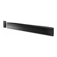
SA-VE812ED/VE815ED/WMS815/SS-MS815
33
SECTION 1
GENERAL
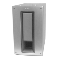
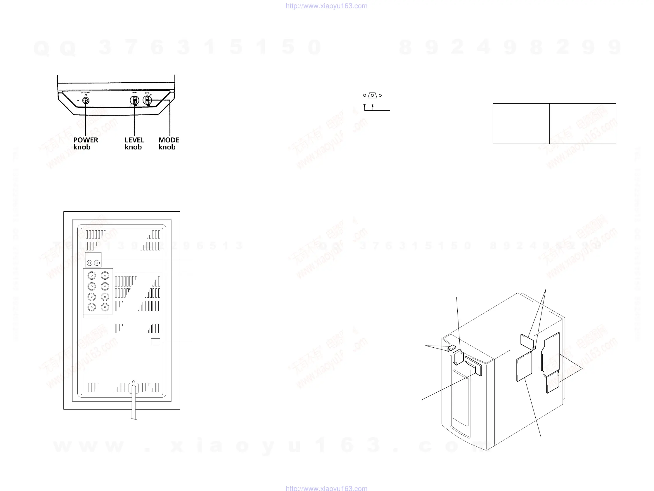
• Location of Controls
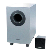
SA-WMS7
– Front view –
– Rear view –
SECTION 2
DIAGRAMS
2-1. NOTE FOR PRINTED WIRING BOARDS AND SCHEMATIC DIAGRAMS
Note on Printed Wiring Board:
• X : parts extracted from the component side.
• b : Pattern from the side which enables seeing.
(The other layers' patterns are not indicated.)
• Indication of transistor.
Note on Schematic Diagram:
• All capacitors are in µF unless otherwise noted. pF: µµF
50 WV or less are not indicated except for electrolytics
and tantalums.
• All resistors are in Ω and
1
/
4
W or less unless otherwise
specified.
• 2 : nonflammable resistor.
• C : panel designation.
• U : B+ Line.
• V : B– Line.
• Voltages are dc with respect to ground under no-signal
conditions.
no mark : AUDIO
• Voltages are taken with a VOM (input impedance 10 MΩ).
Voltage variations may be noted due to normal produc-
tion tolerances.
• Signal path.
F : AUDIO
• Abbreviation
CND : Canadian model
G : German model
MY : Malaysia model
SP : Singapore model
Note:
The components identi-
fied by mark ! or dotted
line with mark ! are criti-
cal for safety.
Replace only with part
number specified.
Note:
Les composants identifiés par
une marque ! sont critiques
pour la sécurité.
Ne les remplacer que par une
piéce portant le numéro
spécifié.
• Circuit Boards Location
SA-WMS815
LINE IN/OUT jack
SPEAKER IN/OU
terminal
POWER SAVE
switch
POWER SWITCH board
POWER board
LED board
CONTROL board
AUTO POWER board
MAIN boar
w
w
w
.
x
i
a
o
y
u
1
6
3
.
c
o
m
Q
Q
3
7
6
3
1
5
1
5
0
9
9
2
8
9
4
2
9
8
T
E
L
1
3
9
4
2
2
9
6
5
1
3
9
9
2
8
9
4
2
9
8
0
5
1
5
1
3
6
7
3
Q
Q
TEL 13942296513 QQ 376315150 892498299
TEL 13942296513 QQ 376315150 892498299
http://www.xiaoyu163.com
http://www.xiaoyu163.com
 Loading...