4
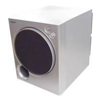
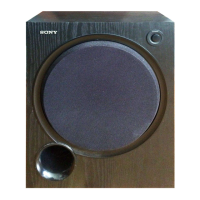
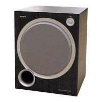
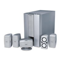
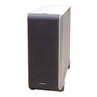
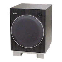
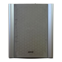
SA-WMS145/WMSP50
Note on Schematic Diagram:
• All capacitors are in µF unless otherwise noted. pF: µµF
50 WV or less are not indicated except for electrolytics
and tantalums.
• All resistors are in Ω and
1
/
4
W or less unless otherwise
specified.
• 2 : nonflammable resistor.
• C : panel designation.
• A : B+ Line.
• B : B– Line.
•Voltage is dc with respect to ground under no-signal
(detuned) condition.
•Voltages are taken with a VOM (Input impedance 10 MΩ).
Voltage variations may be noted due to normal produc-
tion tolerances.
• Signal path.
F : AUDIO
Note on Printed Wiring Boards:
• X : parts extracted from the component side.
• : Pattern from the side which enables seeing.
Note: The components identified by mark 0 or dotted line
with mark 0 are critical for safety.
Replace only with part number specified.
Ref. No. Location
D205 E-10
D206 E-11
D301 G-7
D302 G-8
D304 E-9
D401 D-6
D402 D-7
D403 D-7
D501 D-8
D502 G-7
D602 D-10
D901 A-10
IC202 E-11
IC203 E-12
IC301 G-9
Q501 D-9
Q502 D-9
Q503 D-10
Q504 D-10
Q505 G-7
• Semiconductor
Location