39
STR-KS600PM/KS600PW
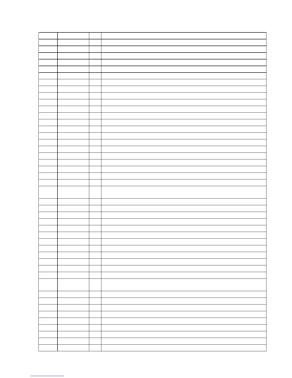
Pin No.
Pin Name
I/O
Description
52
RDS CLK
I
RDS interrupt clock signal input from the tuner unit
53
RDS DATA
I
RDS serial data input from the tuner unit
54
SIRCS
I
SIRCS signal input terminal
55
FUSE DETECT
I
Fuse open detection signal input terminal "L": fuse opened
56
POWER KEY
I
Power key input terminal "L": switch on
57
NO USE
-
Not used
58 to 60
LAT3 to LAT1
O
Latch signal output to the stream processor
61
SHIFT
O
Serial data latch pulse output to the stream processor
62
SCDT
O
Serial data output to the stream processor
63
SOFT_MUTE
O
Muting on/off control signal output terminal
64
INT
O
Initialize signal output to the stream processor
65
STEREO
I
FM stereo detection signal input from the FM/AM tuner pack
66
TUNED
I
Tuned detection signal input from the FM/AM tuner pack
67
TUNER_LED
O
LED drive signal output terminal
68
OVF
I
Overflow signal input from the stream processor
69
FAN_CTL
O
Fan motor on/off control signal output terminal Not used
70, 71
VOLB, VOLA
I
Jog dial pulse input terminal
72
FL_DATA
O
Serial data output to the fluorescent display tube driver
73
FL_CLK
O
Serial data transfer clock signal output to the fluorescent indicator tube driver
74
FL_STB
O
Strobe signal output to the fluorescent indicator tube driver
75
FAN_CLK
I
Fan motor feedback clock signal input terminal Not used
76
FAN_ON
I
Fan motor level detection signal input terminal Not used
77
RSTX
I
System reset signal input from the reset signal generator "L": reset
For several hundreds msec. after the power supply rises, "L" is input, then it changes to "H"
78
OVFW
I
Overflow signal input for subwoofer from the stream processor
79
X1A
O
Sub system clock output terminal Not used
80
X0A
I
Sub system clock input terminal Not used
81
VSS
-
Ground terminal
82
X0
I
Main system clock input terminal (24 MHz)
83
X1
O
Main system clock output terminal (24 MHz)
84
VCC3
-
Power supply terminal (+3.3V)
85
T. CLK
O
Serial data transfer clock signal output to the FM/AM tuner pack
86
T. DATA
O
Serial data output to the FM/AM tuner pack
87
SLATCH
O
Latch signal output to the FM/AM tuner pack
88
T_DO
I
Serial data input from the FM/AM tuner pack
89
T_MUTE
O
Muting on/off control signal output terminal
90, 91
TC74AC_A,
TC74AC_B
-
Not used
92
LRCK_SW
O
L/R sampling clock signal switching signal output terminal
93
XMODE
O
System reset signal output to the digital audio interface receiver "L": reset
94
CKSEL1
O
Output clock selection signal output terminal Not used
95
CLK
O
Clock signal output to the digital audio interface receiver
96
CE
O
Chip enable signal output to the digital audio interface receiver
97
D1
O
Write data output to the digital audio interface receiver
98
D0
I
Read data input from the digital audio interface receiver
99
ERROR
I
PLL lock error signal and data error flag input from the digital audio interface receiver
100
XSTATE
I
Source clock selection monitor input from the digital audio interface receiver


 To Next Page