EasyManua.ls Logo

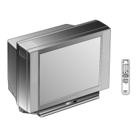
Sony TRINITRON KV-29FV300 - Block Diagram and Schematics

Sony TRINITRON KV-29FV300
205 pages
Print Icon
To Next Page IconTo Next Page
To Previous Page IconTo Previous Page
Loading...
— 30 —
KV-27FV300/29FV300/32FV300/36FV300
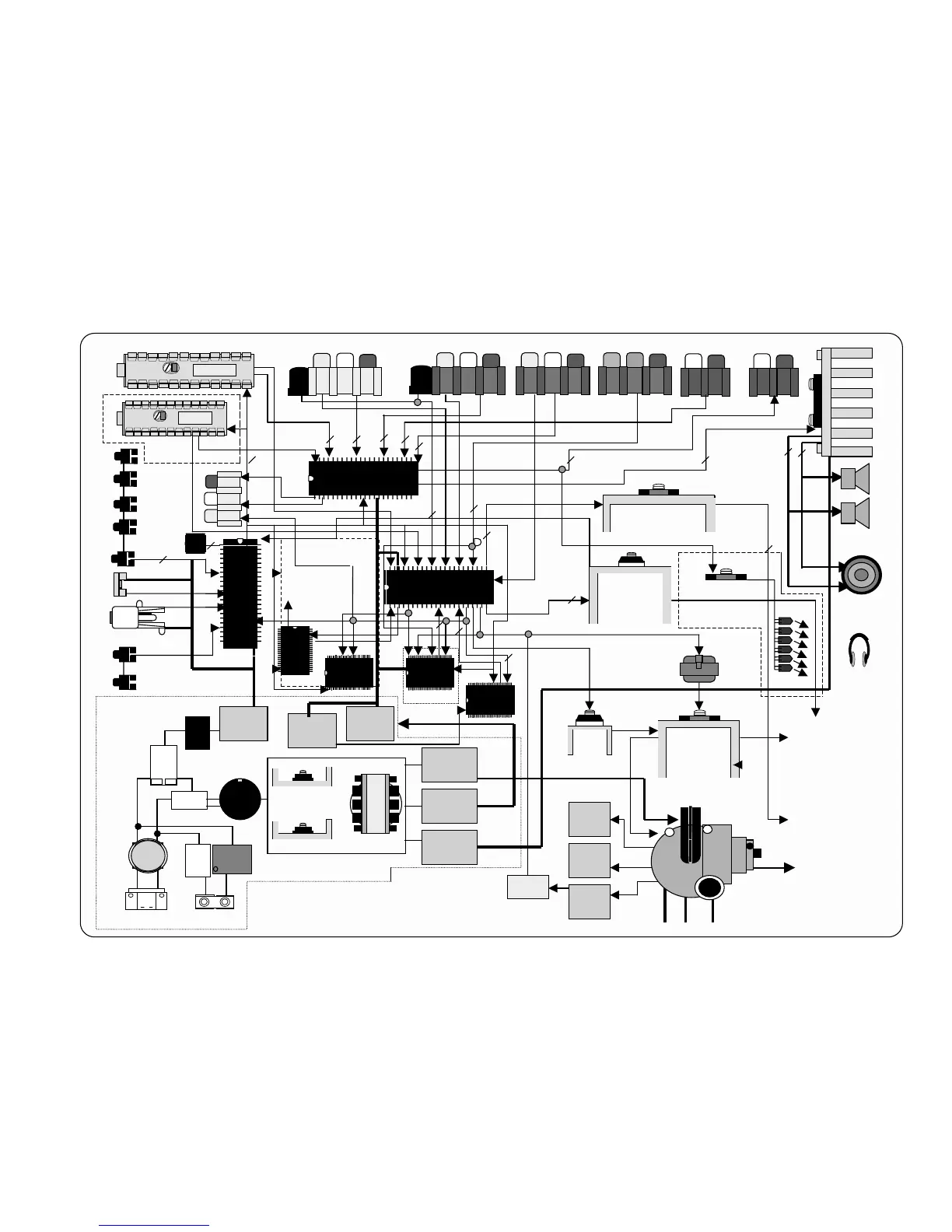
5-3. BLOCK DIAGRAM AND SCHEMATICS
TV-8
V-Out
AN5522 (24-27”)
STV9379(32-36”)
L.E.D.
Menu
CTRL
I.R.
H-Out
2SD2634(27”)
2SD2645(32-36”)
DEC
5VDC
TV-8
D.G.C.
AC Line
L.F.T
LR
Tuner FRONT
V2 LR
AUDIO OUT
H.Drive
Energy Star
Relay
THP
Rect.
2
2
2
2
S
4
Audio Amplifier
TDA8580J
10W&15W
2
I2C Bus
2
Vd
Hp
E/W
2
Power Supply
5V
Reg.
5V
STBY
SRT
Power Mosfet
2SK2876
Audio Processor
NJW1134
Pin
Out
2SC4159
+13v
Rect.
-13v
Rect.
OCP
Horiz.
Vert.
Speakers
2
R
L
IR Head
phones
2
2
Low B
Rect.
Audio
Rect.
B+
Rect.
135V
G2
HV
Focus
Y/C
Sub det-Out
24V
12.5V
200v
Rect.
FBT
FBT
3 RGB
3RGB
V1 LR
REAR
LR
YUV AUDIOYUV
Y UV
3
2
Mircoprocessor
M306V5ME
Video processor
CXA2154/5AS
27”-NX4521
32-36”-NX4600
2
CVBS,FSC
2
Y/C
3L comb
TC90A69.
For FS only
3
YUV
PinP Proc.
M65665FP.
P board
Iprot
G board
3D comb
MN82832.
C
Yout
BC board
Sub woofer
(for FV only)
9V
Reg.
Tuner
L
S
P board
Det. out
REAR
V3 LR
2
(For FV only)
RGB Driver
TDA6108
IR modulator
BA3308
Emiter
T board
2
SRT
TA1226N
Yin
V
L
R
MOUT
To DY
To CRT
To CRT

Table of Contents