○○○○○○○○○○○○○○○○○○○○○○○○○○○○○○○○○○○○○○○○○○○○○○○○○○○○○○○○○○○○○○○○○○○○○○○○○○○○○○○○○○○○○○○○○○○○○○○○○○○○○○○○○○
○○○○○○○○○○○○○○○○○○○○○○○○○○○○○○○○○○○○○○○○○○○○○○○○○○○○○○○○○○○○○○○○○○○○○○○○○○○○○○○○○○○○○○○○○○○○○○○○○○○○○○○○○○
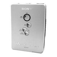
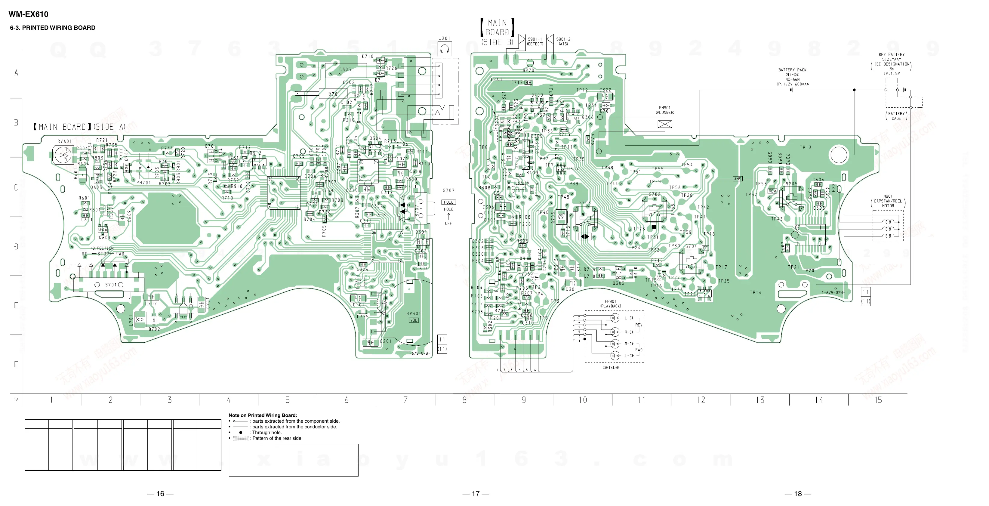
WM-EX610
— 16 — — 17 — — 18 —
6-3. PRINTED WIRING BOARD
Note on Printed Wiring Board:
• X : parts extracted from the component side.
• Y : parts extracted from the conductor side.
•
r
: Through hole.
• b : Pattern of the rear side.
Caution:
Pattern face side: Parts on the pattern face side seen from
(SIDE B) the pattern face are indicated.
Parts face side: Parts on the parts face side seen from
(SIDE A) the parts face are indicated.
• Semiconductor Location
Ref. No. Location
IC301 D-7
IC302 C-6
IC601 C-14
IC701 C-5
IC702 E-3
IC703 C-5
IC704 E-12
Ref. No. Location
D701 B-10
D702 E-3
D703 C-10
D709 B-9
D710 A-7
D711 A-7
Ref. No. Location
Q301 D-7
Q302 C-9
Q303 C-9
Q304 B7
Q305 D-11
Q306 B-10
Q307 C-10
Ref. No. Location
Q603 C-2
Q604 D-2
Q701 B-4
Q702 C-2
FR
EXCEPT
FR
V
VCC
DATA
REMO
GND
RCH
COM
LCH
w
w
w
.
x
i
a
o
y
u
1
6
3
.
c
o
m
Q
Q
3
7
6
3
1
5
1
5
0
9
9
2
8
9
4
2
9
8
T
E
L
1
3
9
4
2
2
9
6
5
1
3
9
9
2
8
9
4
2
9
8
0
5
1
5
1
3
6
7
3
Q
Q
TEL 13942296513 QQ 376315150 892498299
TEL 13942296513 QQ 376315150 892498299
http://www.xiaoyu163.com
http://www.xiaoyu163.com
 Loading...