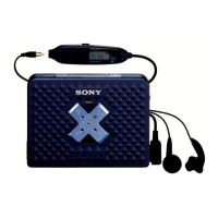
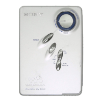
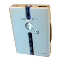
WM-EX651
1212
WM-EX651
For schematic diagrams.
Note:
• All capacitors are in µF unless otherwise noted. (p: pF)
50 WV or less are not indicated except for electrolytics
and tantalums.
•%: indicates tolerance.
• C : panel designation.
• A : B+ Line.
• H : adjustment for repair.
• Power voltage is dc 1.5 V and fed with regulated dc power
supply from battery terminal.
no mark : PLAY
•Voltages and waveforms are dc with respect to ground in
playback mode.
•Waveforms are taken with a oscilloscope.
Voltage variations may be noted due to normal produc-
tion tolerances.
• Circled numbers refer to waveforms.
• Signal path.
E : PB
NOTE FOR PRINTED WIRING BOARDS AND SCHEMATIC DIAGRAMS.
Caution:
Parts face side: Parts on the parts face side seen from
(Side A) the parts face are indicated.
Pattern face side: Parts on the pattern face side seen from
(Side B) the pattern face are indicated.
For printed wiring boards.
Note:
• X : parts extracted from the component side.
• x : parts extracted from the conductor side.
•
®
: Through hole.
• : Pattern from the side which enables seeing.
6-1. IC BLOCK DIAGRAMS
IC301 TA2123AF (EL)
 Loading...