17
WM-GX400
Common Note on Schematic Diagram:
• All capacitors are in µF unless otherwise noted. pF: µµF
50 WV or less are not indicated except for electrolytics
and tantalums.
• All resistors are in Ω and
1
/
4
W or less unless otherwise
specified.
• C : panel designation.
• A : B+ Line.
• H : adjustment for repair.
• Power voltage is dc 3V and fed with regulated dc power
supply from battery terminal.
• Voltage and waveforms are dc with respect to ground
under no-signal (detuned) conditions.
no mark : FM
( ) : AM
<< >> : REC
[ ] : PB
• Voltages are taken with a VOM (Input impedance 10 MΩ).
Voltage variations may be noted due to normal produc-
tion tolerances.
• Waveforms are taken with a oscilloscope.
Voltage variations may be noted due to normal produc-
tion tolerances.
• Circled numbers refer to waveforms.
• Signal path.
F : FM
f : AM
E : PB
a : REC
N : MIC
• Abbreviation
CND : Canadian
FR : French
EA : Saudi Arabia
CH : Chinese
JEW : Tourist
E : Indication of country of origin (ST, MONO)
9E : No Indication of country of origin
5E : Indication of country of origin (DX, LOCAL)
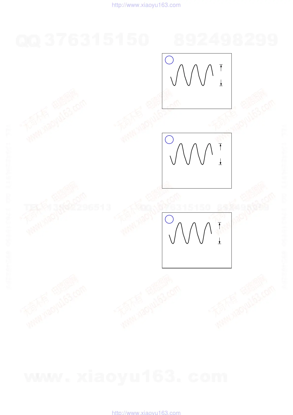
1
IC401 C
VOLT/DIV : 0.5 V AC
TIME/DIV : 0.1 µsec
– MAIN SECTION (1/2) –
z
Waveforms
RADIO mode
3.2Vp-
26MHz
2
Q334 C
VOLT/DIV : 0.5 V AC
TIME/DIV : 10 µsec
– MAIN SECTION (2/2) –
REC mode
2.9Vp-p
48KHz
3
IC701 1
XOUT
VOLT/DIV : 50 mV AC
TIME/DIV : 5 µsec
– DISPLAY SECTION –
265mVp-
75KHz
w
w
w
.
x
i
a
o
y
u
1
6
3
.
c
o
m
Q
Q
3
7
6
3
1
5
1
5
0
9
9
2
8
9
4
2
9
8
T
E
L
1
3
9
4
2
2
9
6
5
1
3
9
9
2
8
9
4
2
9
8
0
5
1
5
1
3
6
7
3
Q
Q
TEL 13942296513 QQ 376315150 892498299
TEL 13942296513 QQ 376315150 892498299
http://www.xiaoyu163.com
http://www.xiaoyu163.com
 Loading...