3-5
SR830 Basics
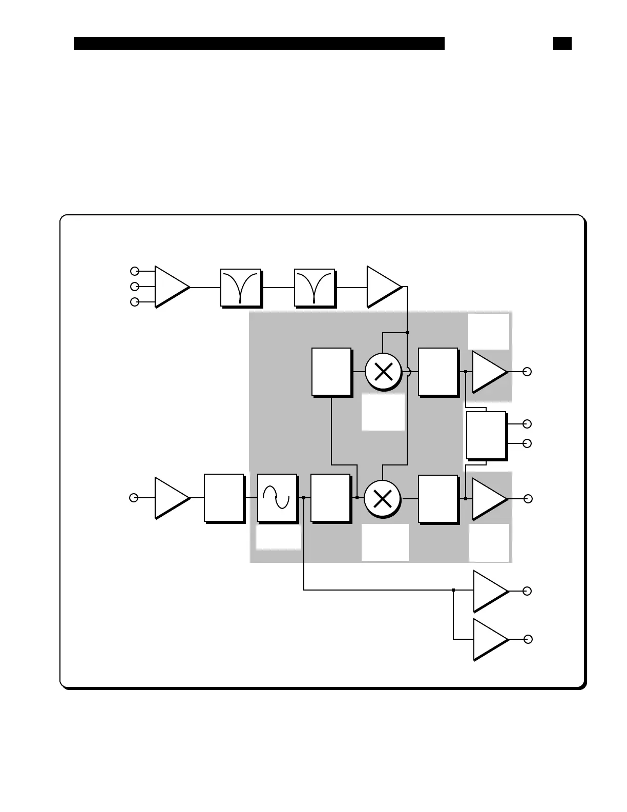
The functional block diagram of the SR830 DSP
Lock-In Amplifier is shown below. The functions in
the gray area are handled by the digital signal pro-
cessor (DSP). We'll discuss the DSP aspects of
the SR830 as they come up in each functional
block description.
THE FUNCTIONAL SR830
Phase
Sensitive
Detector
PLL
I
A
B
Low Noise
Voltage
Current
50/60 Hz
Notch
Filter
Reference In
Sine or TTL
Phase
Shifter
DC Gain
Offset
Expand
Gain
X Out
Y Out
Discriminator
90°
Phase
Shift
Phase
Internal
Oscillator
Low
Pass
Filter
DC Gain
Offset
Expand
Low
Pass
Filter
Sine Out
Discriminator
TTL Out
R and
Ø Calc
R
Ø
Phase
Sensitive
Detector
SR830 FUNCTIONAL BLOCK DIAGRAM