M850-00
T856/857 Circuit Operation
C2.5
Copyright TEL 31/09/98
2.3 Synthesised Local Oscillator
(Refer to the synthesiser circuit diagram (sheet 7) in Section 6.2 or 6.3 and the VCO cir-
cuit diagram in Part E.)
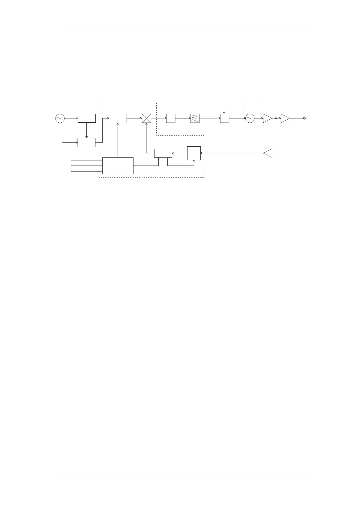
Figure 2.4 T856/857 Synthesiser Block Diagram
The synthesiser (IC740) employs a phase-locked loop (PLL) to lock a voltage controlled
oscillator (VCO) to a given reference frequency. The synthesiser receives the divider
information from the control microprocessor via a 3 wire serial bus (clock, data, enable).
When the data has been latched in, the synthesiser processes the incoming signals from
the VCO buffer (f
in
) and the phase modulator (f
ref
).
A reference oscillator at 12.8MHz (=IC700) is buffered (IC710 pins 3 & 4) and divided
down to 200kHz (IC730). This 200kHz square wave is then summed with the modulat-
ing audio and passed to an integrator (IC720 pins 9 & 8, Q710, Q720). This produces a
ramping waveform which is centred around a DC level determined by the incoming
audio. IC720 pins 5 & 6 perform as a comparator, ultimately producing a phase-modu-
lated 200kHz square wave. This is followed by another phase shifting stage (IC720 pins
3 & 4, Q730, Q740), before being divided down to 6.25kHz or 5kHz within the synthe-
siser IC (IC740).
A buffered output of the VCO (Q795) is divided with a prescaler and programmable
divider which is incorporated into the synthesiser chip (IC740). This signal is compared
with the phase modulated reference signal at the phase detector (also part of the synthe-
siser chip). The phase detector outputs drive a balanced charge pump circuit (Q760,
Q770, Q775, Q780, Q785) and active loop filter (IC750 pins 5, 6 & 7, Q790) which pro-
duces a DC voltage between 0V and 20V to tune the VCO. This VCO control line is fur-
ther filtered to attenuate noise and other spurious signals. Note that the VCO frequency
increases with increasing control voltage.
If the synthesiser loop loses lock, a pulsed signal appears at LD (pin 2) of IC740. This
signal is filtered and buffered by IC750 pins 1, 2 & 3, producing the Lock-Detect signal
used to shut off the power supply to the drive amplifier. IC750 pin 1 is at 20V when the
synthesiser is out of lock.
/R
Reference
Divider
12.8MHz
Reference
Oscillator
Fixed
Divider
/64
Phase
Modulator
Ref
Mod
Phase
Detector
Charge
Pump
Loop
Filter
FREQUENCY SYNTHESISER IC
Serial
Bus
Clk
Data
En
Controller
/N
Programmable
Divider
64/65
Prescaler
VCO PCB
VCO
Modulation
VCO Buffer
Output
Buffer
+22dB
L.O.
Divider Buffer
f
ref
f
in
Σ