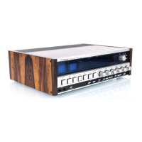
Do you have a question about the TANDBERG TR 2075 Mk II and is the answer not in the manual?
| Power output | 75 watts per channel into 8Ω (stereo) |
|---|---|
| Speaker load impedance | 4Ω to 16Ω |
| Tuning range | 87.5 - 108 MHz |
| Frequency response | 20Hz to 20kHz |
| Input sensitivity | 150mV (line) |
| Signal to noise ratio | 90dB (line) |
Instructions for cleaning and lubricating push button switches.
Step-by-step guide for disassembling the plunger mechanism.
Procedure for replacing output transistors and heat sink.
Guide for fitting and routing the scale drive cord.
Detailed steps for aligning AM-IF, antenna, and signal meter circuits.
Schematic diagram of the AM Tuner board (A4).
Steps for aligning FM tuner, discriminator, and stereo decoder.
Schematic diagram of the FM Tuner board (A1).
Schematic diagram of the FM IF and Decoder board (A2).
Schematic diagram of the RIAA/Input Amplifier board (A5).
Schematic diagram of the Preamplifier board (A7).
Schematic diagram of the Program Select/Voltage Regulator board (A6).
Schematic diagram of the Mode/Filter board (A8).
Schematic diagram of the Power Amplifier board (A9).
Procedure for power reading and quiescent current adjustment.