M
PD765A/
M
PD7265
SEC
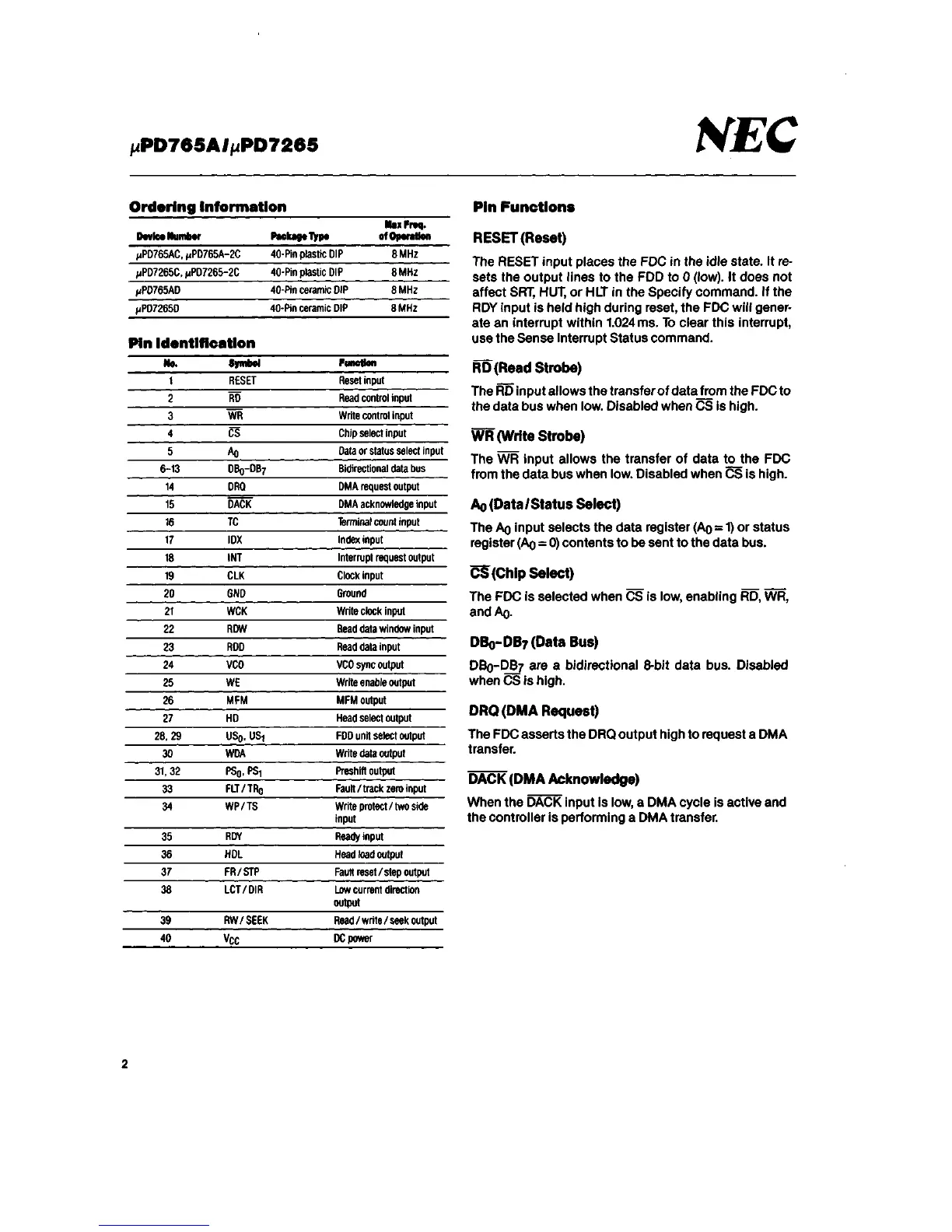
Ordering Information
D^Humbor
H
PD765AC,
M
PD765A-2C
M
PD7265C,
M
PD7265-2C
MPD765AD
M
PD7265D
Pin Identification
No.
1
2
3
4
5
6-13
14
15
16
17
18
19
20
21
22
23
24
25
26
27
28,29
30
31,32
33
34
35
36
37
38
39
40
Symbol
RESET
RD
WR
CS
Ao
DB
0
-DB
7
DRQ
DACK
TC
IDX
INT
CLK
GND
WCK
RDW
RDD
VCO
WE
MFM
HD
US
0
.
USi
WDA
PS
0
,
PS1
FLT/TRo
WP/TS
RDY
HDL
FR/STP
LCT/DIR
RW/SEEK
Vcc
MaxPraq.
Packagolyp* ofOporation
40-Pin plastic DIP 8 MHz
40-Pin plastic DIP 8 MHz
40-Pin ceramic DIP 8 MHz
40-Pin ceramic DIP 8 MHz
Function
Reset input
Read control input
Write control input
Chip select input
Data
or status select input
Bidirectional data bus
DMA request output
DMA acknowledge input
Terminal count input
Index input
Interrupt request output
Clock input
Ground
Write clock input
Bead data window input
Read data input
VCO
sync output
Write enable output
MFM output
Head select output
FDD unit select output
Write data output
Preshift output
Fault/track zero input
Write protect/two side
input
Ready input
Head
load
output
Fault reset /step output
Low current direction
output
Read/write/seek output
DC
power
Pin Functions
RESET (Reset)
The RESET input places the FDC in the idle state. It re-
sets the output lines to the FDD to 0 (low). It does not
affect
SRT, HUT,
or HLT in the Specify
command.
If the
RDY input is held high during reset, the FDC will
gener-
ate an interrupt within 1.024
ms.
To clear this interrupt,
use the Sense Interrupt Status command.
RD
(Read Strobe)
The
RD
input allows
the
transfer of
data_from
the
FDC
to
the data bus
when
low. Disabled when CS is
high.
WR (Write Strobe)
The WR input allows the transfer of data tojhe FDC
from the data bus when low. Disabled when CS is
high.
Ao (Data/Status Select)
The Ao input selects the data register
(Ao
=
1)
or status
register
(Ao
=
0)
contents to be sent to the data bus.
CS (Chip Select)
The FDC is selected when CS is low, enabling
RD,
WR,
andAo-
DB0-DB7 (Data Bus)
DB0-DB7 are a bidirectional
8-bit
data bus. Disabled
when
CS
is
high.
DRQ (DMA Request)
The
FDC
asserts the
DRQ
output high to request a DMA
transfer.
DACK (DMA Acknowledge)
When the DACK input is low, a DMA cycle is active and
the controller is performing a DMA transfer.