•
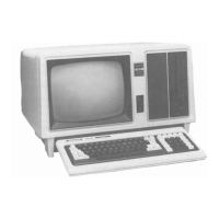
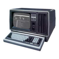
TANDY COMPUTER PRODUCTS •
Bus Interface
The interface to the main bus is divided into three parts:
address/control strobes, memory data and I/O data.
The
address/control strobe part (AO
-
A19, MEMR*, MEMW*, IOR*,
IOW*) is shared by both the I/O and the memory sections.
The address buffers are U23, U32 and U36. One function of
the address bus is the select logic for each of the
functions.
U27 decodes all the I/O chip selects except
those for the Video/System Memory I/O ports which are
decoded by U31. The memory selects are decoded by U31 except
the ROMCS*, which is decoded by U16. The I/O data
transceiver is U44 with its output enable and direction
control decoded by U16.
Keyboard
/
Timer
/
Sound Circuits
The Keyboard Interface consists of an 8048 CPU (U9) and
a
Keyboard Controller
(U13),
which is
a
Custom Gate Array.
Included in U13 is an 8255 programmable peripheral interface
equivalent design. It has three
8
bit parallel ports, A,
B
and C. Port
A
is configured as an input port and is used
for keyboard data. Port
B
is configured as an output port
and is used for control signals for the sound, keyboard and
timer functions. Port
C
is split into 4 inputs, including
the timer channel and #2 monitor and 4 outputs including the
keyboard/multifunction interface signals.
The 8048 generates strobes to the keyboard. Data from the
keyboard is received by the
8048,
translated to an
8
bit
asynchronous serial format, and transmitted to the Keyboard
Controller. The Keyboard Controller translates this serial
data into
a
parallel format and makes it available to the
data bus. The serial data from the 8048 consists of
a
clock
signal and
a
data signal. The clock consists of
8
consecutive positive pulses (signal normal state is logic
low).
The rising edge of each pulse is centered in the
middle of each data period. The data signals consists of
8
data periods and an "end-of-character" bit. Normal state of
the data signal is logic high which represents
a
logic 1.
Thus,
the data signal will change only if the data bit is
a
0. The ninth and last data bit is always
a
0. In the
absence of
a
ninth clock, it will set the interrupt and busy
signals.
See Figure 9 for the Keyboard Timing Chart.
30