8088
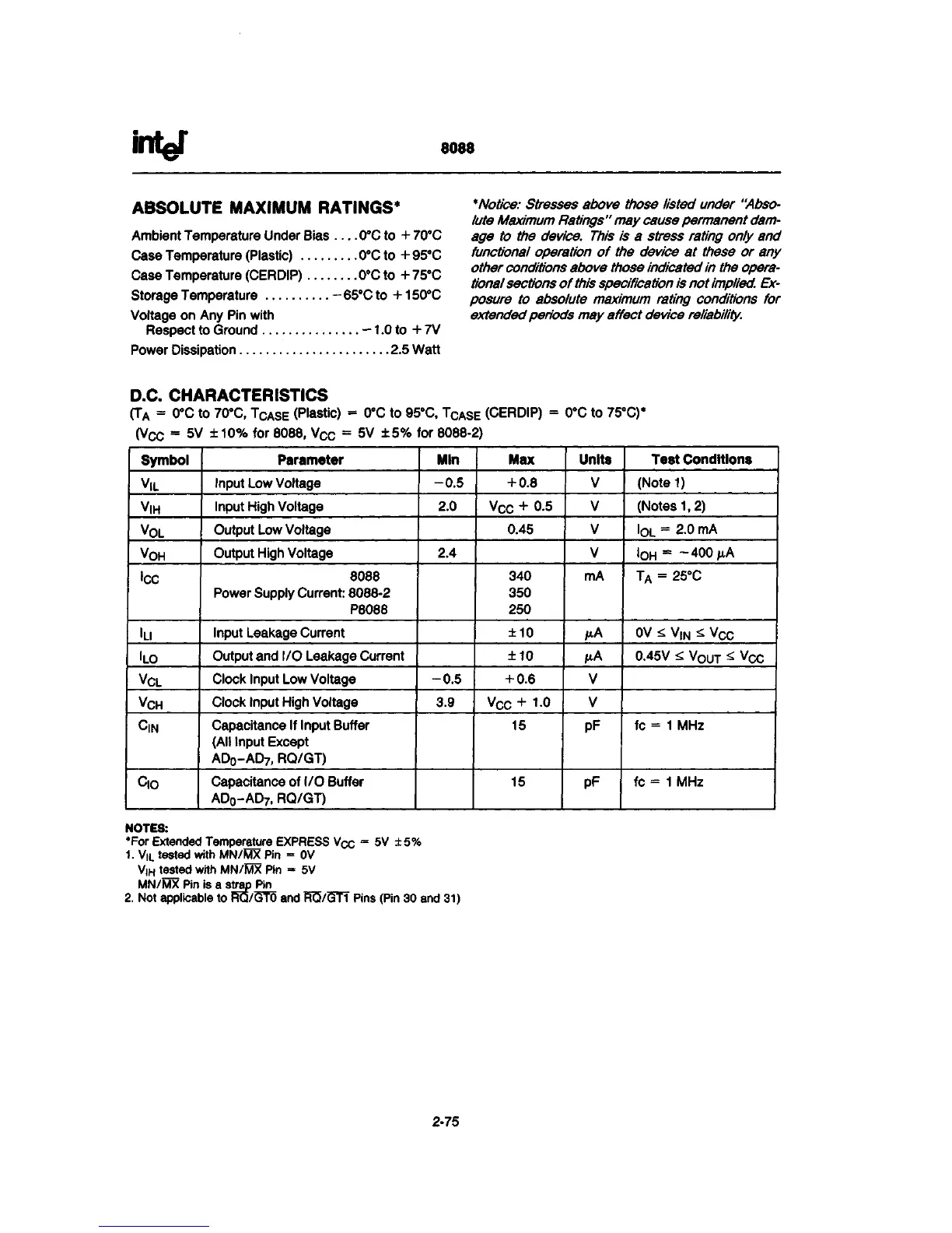
ABSOLUTE MAXIMUM RATINGS*
Ambient Temperature Under Bias ... .0°C to + 70°C
Case Temperature (Plastic) 0°C to + 95°C
Case Temperature (CERDIP) 0°C to + 75°C
Storage Temperature - 65°C to +150°C
Voltage on Any Pin with
Respect to Ground -1.0 to +7V
Power Dissipation 2.5 Watt
* Notice: Stresses above those listed under "Abso-
lute
Maximum
Ratings" may
cause
permanent
dam-
age to the device. This is a stress rating only and
functional operation of the device at these or any
other
conditions
above those indicated in the
opera-
tional sections of this specification is not
implied.
Ex-
posure to absolute maximum rating conditions for
extended periods may affect device
reliability.
D.C. CHARACTERISTICS
(TA
= 0°C to 70°C,
TCASE
(Plastic) = 0°C to 95°C,
T
CA
SE
(CERDIP) = 0°C to 75°C)*
(V
C
c = 5V ±10% for 8088, V
C
c = 5V ±5% for 8088-2)
Symbol
V|L
V|H
V
0
L
V
0
H
»CC
»LI
ILO
V
C
L
V
C
H
QN
c,
0
Parameter
Input Low Voltage
Input High Voltage
Output Low Voltage
Output High Voltage
8088
Power Supply Current: 8088-2
P8088
Input Leakage Current
Output and I/O Leakage Current
Clock Input Low Voltage
Clock Input High Voltage
Capacitance If Input Buffer
(All Input Except
AD
0
-AD
7
,
RQ/GT)
Capacitance of I/O Buffer
AD0-AD7, RQ/GT)
Mln
-0.5
2.0
2.4
-0.5
3.9
Max
+ 0.8
V
C
c + 0.5
0.45
340
350
250
±10
±10
+ 0.6
v
C
c+ 10
15
15
Units
V
V
V
V
mA
JLlA
JLtA
V
V
PF
PF
Test Conditions
(Notel)
(Notes 1,2)
IOL
=
2.0 mA
I
OH
=
-400 |aA
T
A
= 25°C
0V £ V,
N
£ V
CC
0.45V
<;
VQUT
^ V
CC
fc =
1
MHz
fc =
1
MHz
NOTES:
*For Extended
Temperature
EXPRESS
Vcc = 5V ±5%
1.
V|
L
tested
with
MN/MX
Pin = 0V
V|
H
tested
with
MN/MX
Pin - 5V
MN/MX
Pin is a
strap
Pin
2. Not
applicable
to
RQ/STO
and
RT5/5TT
Pins
(Pin 30 and 31)
2-75
 Loading...