STMicroelectronics Confidential 3/14
STV8172A Electrical Characteristics
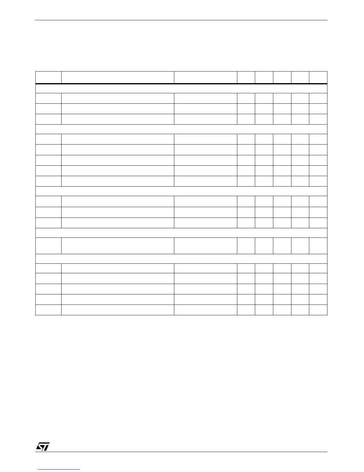
3 Electrical Characteristics
(V
S
= 34 V, T
AMB
= 25°C, unless otherwise specified)
8. In normal applications, the peak flyback voltage is slightly greater than 2 x (V
S
- V
4
). Therefore, (V
S
- V
4
) = 35 V is not allowed without special circuitry.
9. Refer to Figure 4, Stand-by condition.
Symbol Parameter Test Conditions Min. Typ. Max. Unit Fig.
Supply
V
S
Operating Supply Voltage Range (V
2
-V
4
) Note 8 10 35 V
I
2
Pin 2 Quiescent Current I
3
= 0, I
5
= 0 5 20 mA 1
I
6
Pin 6 Quiescent Current I
3
= 0, I
5
= 0, V
6
=35v 8 19 50 mA 1
Input
I
1
Input Bias Current V
1
= 1 V, V
7
= 2.2 V - 0.6 -1.5 µA1
I
7
Input Bias Current V
1
= 2.2 V, V
7
= 1 V - 0.6 -1.5 µA
V
IR
Operating Input Voltage Range 0 V
S
- 2 V
V
I0
Offset Voltage 2mV
DV
I0
/dt Offset Drift versus Temperature 10 µV/°C
Output
I
0
Operating Peak Output Current
0
o
<Tcase<125
o
C
±1.5
A
V
5L
Output Saturation Voltage to pin 4 I
5
= 1.5 A 1 1.7 V 3
V
5H
Output Saturation Voltage to pin 6 I
5
= -1.5 A 1.8 2.3 V 2
Stand-by
V
5STBY
Output Voltage in Stand-by
V
1
= V
7
= V
S
= 0
See Note 9
V
S
- 2
V
Miscellaneous
G Voltage Gain 80 dB
V
D5-6
Diode Forward Voltage Between pins 5-6 I
5
= 1.5 A 1.8 2.3 V
V
D3-2
Diode Forward Voltage between pins 3-2 I
3
= 1.5 A 1.6 2.2 V
V
3SL
Saturation Voltage on pin 3 I
3
= 20 mA 0.4 1 V 3
V
3SH
Saturation Voltage to pin 2 (2nd part of flyback) I
3
= -1.5 A 2.1 2.8 V
 Loading...