EasyManua.ls Logo

Technics SU-X933

Technics SU-X933
23 pages
To Next Page IconTo Next Page
Loading...
ORDER
NO.
AD8904097C8
.
Manual
Amplifier
SU-X933
Color
(K)...Black
Type
Area
Country
ee
ae
Service
Digital
Integrated
Amplifier
SPECIFICATIONS
(DIN
45
500)
AMPLIFIER
SECTION
Muting
—20
dB
Super
bass
70
Hz,
O~
+10
dB
DIN
power
output
Output
voltage
1kHz
THD:
1%
2x50
W
(8
Q)
TAPE
REC
OUT
200
mV
Total
harmonic
distortion
Channel
balance,
AUX
250
Hz~-6,300
Hz
+1.0
dB
rated
power
at
1
kHz
1%
(8Q)
Channel
separation,
AUX
1
kHz
55
dB
Harmonic
distortion
Headphones
output
level
and
impedance
473
mV/330
Q
half
power
at
1
kHz
0.03
%
(8Q)
Load
impedance
Residual
hum
and
noise
0.5
mV
MAIN
8N~16Q
Damping
factor
30
(8
Q)
SURROUND
8Q~16N
Input
sensitivity
and
impedance
PHONO
3
mV/47
kQ
TUNER,
AUX,
TAPE
200
mV/22
kQ
i
GENERAL
cD
300
mv/15
kQ
Maximum
input
voltage
(1
kHz,
RMS)
Power
consumption
330
W
PHONO
120
mV
Power
supply
SIN
(rated
power
8
©)
For
Great
Britain
and
New
Zealand
==
AC
50
Hz/60
Hz,
240
V
PHONO
73
dB
(IHF,
A,
79
dB)
For
continental
Europe
AC
50
Hz/60
Hz,
220
V
TUNER,
CD,
AUX,
TAPE
84
dB
(IHF,
A:
83
dB)
For
others
AC
50
Hz/60
Hz,
110
V/127
V/220
V/240
V
Frequency
response
Dimensions
(W
x
H
x
D)
360
x
106.2
x
304
mm
PHONO
RIAA
standard
curve
(14-3/16"
x
4-3/16"
x
12”)
+0.8
dB
(30
Hz~15
kHz)
Weight
5.3
kg
(11.7
Ib.)
TUNER,
CD,
AUX,
TAPE
10
Hz~50
kHz
(—3
dB)
Tone
controls
Notes:
BASS
50
Hz,
+10
dB~—10
dB
1.
Specifications
are
subject
to
change
without
notice.
TREBLE
20
kHz,
+10
dB~—10
dB
Weight
and
dimensions
are
approximate.
2.
Total
harmonic
distortion
is
measured
by
the
digital
spectrum
analyzer.
"Technics
Matsushita
Electric
Industrial
Co.,
Ltd.
,
Central
P.O.
Box
288,
Osaka
530-91,
Japan
Question and Answer IconNeed help?

Do you have a question about the Technics SU-X933 and is the answer not in the manual?

Technics SU-X933 Specifications

General IconGeneral
Power Output100W per channel (8Ω)
Frequency Response5 Hz - 100 kHz
Input Impedance47 kOhms
Dimensions430 x 150 x 380 mm
Input sensitivity150mV (line)
Speaker load impedance4Ω - 16Ω

Summary

Specifications

Amplifier Section Specifications

Detailed electrical and performance specifications for the amplifier section.

General Specifications

Overall specifications including power consumption, dimensions, and weight.

Before Repair Procedures

Protection Circuitry

Explanation of the protection circuit and conditions for its activation.

Accessories

List of included accessories and their area-specific configurations.

Location of Controls

Front Panel Controls

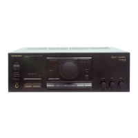
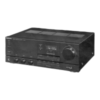
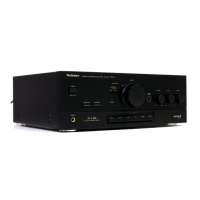
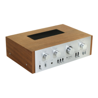
Identification and function of controls on the front panel.

Rear Panel Connections

Identification of input/output terminals and connectors on the rear panel.

Disassembly Instructions

Cabinet and Front Panel Removal

Step-by-step guide for removing the main cabinet and front panel.

Power Switch PCB Removal

Procedure for removing the power switch printed circuit board.

FL DriveTone Amp & Volume PCB Removal

Instructions for removing the FL drive, tone amp, and volume PCBs.

Operation Switch PCB Removal

Procedure for removing the operation switch printed circuit board.

AC OutletAC IN PCB Removal

Instructions for removing the AC outlet and AC IN printed circuit board.

Main PCB and Power IC Removal

Steps for removing the main PCB and power IC or regulator transistor.

Fan Motor and Power Transformer Removal

Procedures for removing the cooling fan motor and power transformer.

Schematic Diagrams

Phono EQ Amp Input Selector Circuit

Schematic for the phono equalizer and input selector circuitry.

InputOutput Terminal Circuit

Schematic detailing the input and output terminal circuitry.

Volume Circuit

Schematic for the electronic volume control circuit.

LEDInput Select Switch Circuit

Schematic for the LED indicators and input selector switch circuit.

Main Circuit Diagram

Overall schematic for the main functional blocks of the amplifier.

Block Diagram

Printed Circuit Boards (PCBs)

Phono EQ AmpInput Selector PCB

Layout diagram for the Phono EQ Amp/Input Selector PCB.

LEDInput Select Switch PCB

Layout diagram for the LED/Input Select Switch PCB.

InputOutput Terminal PCB

Layout diagram for the Input/Output Terminal PCB.

Volume PCB

Layout diagram for the Volume PCB.

FL DriveTone Amp PCB

Layout diagram for the FL Drive/Tone Amp PCB.

Main PCB Layout

Layout diagram for the Main PCB.

AC InAC Outlet Terminal PCB

Layout diagram for the AC In/AC Outlet Terminal PCB.

HeadphonesPower Switch PCB

Layout diagram for the Headphones/Power Switch PCB.

Wiring Connection Diagram

Component Wiring Diagrams

Diagrams showing how components are interconnected.

FL Panel Description

FL Panel Grid Assignment & Pins

Details on FL panel grid layout, pin connections, and anode connections.

FL Panel IC Terminal Functions

Functions of IC terminals related to the FL panel display.

Replacement Parts List

Resistors and Capacitors

List of replacement resistors and capacitors with part numbers.

Integrated Circuits, Transistors, Diodes

List of replacement ICs, transistors, and diodes with part numbers.

Other Components (Oscillators, Switches, Jacks, Fuses)

List of other replacement parts like oscillators, switches, jacks, and fuses.

Exploded View

Service Manual Changes

Transistor and ResistorCapacitor Updates

List of changes made to transistors and resistors/capacitors for performance improvement.

Related product manuals