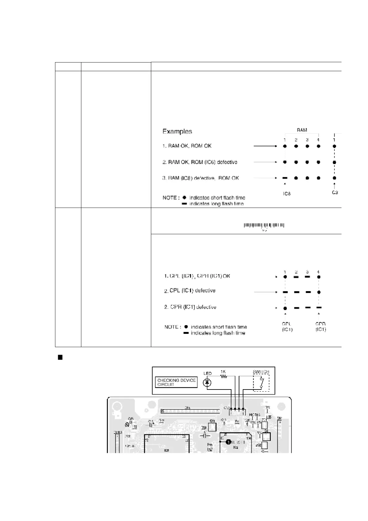
PCB TEST MODE Procedure
MAIN
RAM (IC8), ROM
(IC3,6) check
1. Connect the CHECKING DEVICE to CN3 on the MAIN P.C.B., and turn on the CHECKING
2. Turn on the power switch.
When the power switch is turned on, the LED of the CHECKING
flashes 8 times. The first 4 flashes are for the RAM check, and
flashes are for the ROM check. The order of the LED
the respective IC numbers as shown below. If an IC is defective,
corresponding flash time is longer.
CPL
CPU (IC1) check
1. Connect the CHECKING DEVICE to CN3 on the MAIN P.C.B. (the Checking Device switch
2. Press and hold the two D keys shown below, and then turn on the power switch.
When the power switch is turned on, the LED of the CHECKING
flashes 4 times. The order of the LED flashes correspond to the
on the respective P.C.B.s as shown below. If an IC is defective,
thecorresponding flash time is longer.
Connection between serving CHECKING DEVICE and MAIN P.C.B.