TM 11-6625-2980-14
LIST OF ILLUSTRATIONS
Fig. Page Page
No. No. No.
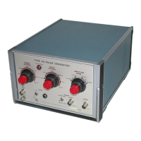
1-0 Pulse Generator AN/USM-359A. vi FO-1 Controls and connectors. 4-1
1-1 PG 508 installation and removal. 1-1 FO-2 Block diagram. 4-3
1-2 Locations of period, delay and duration FO-3 Input circuit schematic diagram. 4-5
custom timing capacitors and TRIG/GATE FO-4 Period generator schematic diagram. 4-7
input impedance switch. 1-2 FO-5 Delay generator schematic diagram. 4-9
1-3 Location for transition custom timing FO-6 Duration generator and control error circuit
capacitor. 1-3 schematic diagram. 4-11
1-4 Equivalent circuit of external input for output FO-7 Transition time generator schematic diagram. 4-13
voltage control. 1-5 FO-8 Level control multiplier schematic diagram.4-15
1-5 Location of trigger jumpers in DD 501 for FO-9 Output amplifier schematic diagram. 4-17
selecting trigger or delay interval output 1-6 FO-10 Tracking voltage supply schematic diagram. 4-19
1-6 PG 508-DD 502 interconnections for counted FO-11 PG 508 power supply schematic diagram. 4-21
burst operation.1-6 FO-12 TM 503 power supply schematic diagram. 4-23
1-7 Typical propagation delays using PG 508 with 5-1 Al board component locations. 5-2
DD 501 in counted burst mode at 50 MHz FO-13 A2 board component locations. 5-3
repetition rate. 1-7 FO-14 A3 board component locations. 5-5
1-8 Pulse characteristics. 1-8 FO-15 A4 board component locations. 5-7
1-9 Locations for user installed rear interface FO-16 PG 508 exploded view. 5-9
connections. 1-12
2-1 Simplified schematic for
control error indicator
logic with control settings
causing illumination. 2-4
iv