EasyManua.ls Logo

Telit Wireless Solutions LM940 - Page 58

Telit Wireless Solutions LM940
75 pages
Print Icon
To Next Page IconTo Next Page
To Previous Page IconTo Previous Page
Loading...
LM940 Hardware Design Guide
1VV0301352 Rev. 18 Page 58 of 75 2022-01-04
Not Subject to NDA
Pin
Signal
I/O
Function
Type
Comment
3
GPIO_01
I/O
General purpose I/O
1.8V
5
GPIO_02
I/O
General purpose I/O
1.8V
44
GPIO_03
I/O
General purpose I/O
1.8V
46
GPIO_04
I/O
General purpose I/O
1.8V
45
GPIO_05
I/O
General purpose I/O
1.8V
47
GPIO_06
I/O
General purpose I/O
1.8V
49
GPIO_07
I/O
General purpose I/O
1.8V
51
GPIO_08
I/O
General purpose I/O
1.8V
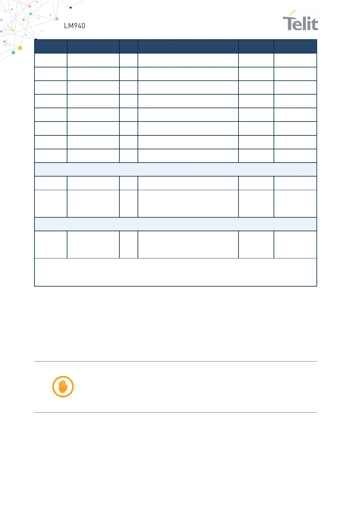
Power ON/OFF Reset IN/OUT
20
W_DISABLE_N
I
Module and RF ON/OFF Control
1.8V
Active Low
*
SYSTEM_RESET_N
I
Reset Input
1.8V
Active Low
See note
1.8V Voltage Regulator
*
VREG_L6_1P8
O
LDO out for 1.8V
Power
See note
Note:
* SIMRST2, SIMVCC2, SYSTEM_RESET_N, VREG_L6_1P8 are assigned differently to LM940 1.0 and 2.0. For more
details refer to the chapter 3. Pins Allocation.
Table 38: EMC Recommendations
All other pins have the following characteristics:
Human Body Model (HBM): ± 1000 V
Charged Device Model (CDM) JESD22-C101-C: ± 250 V
All Antenna pins up to ± 4 kV
Warning: Do not touch without proper electrostatic protective
equipment. The product must be handled with care, avoiding any
contact with the pins because electrostatic discharge may damage
the product itself.