AM1808
SPRS653E –FEBRUARY 2010–REVISED MARCH 2014
www.ti.com
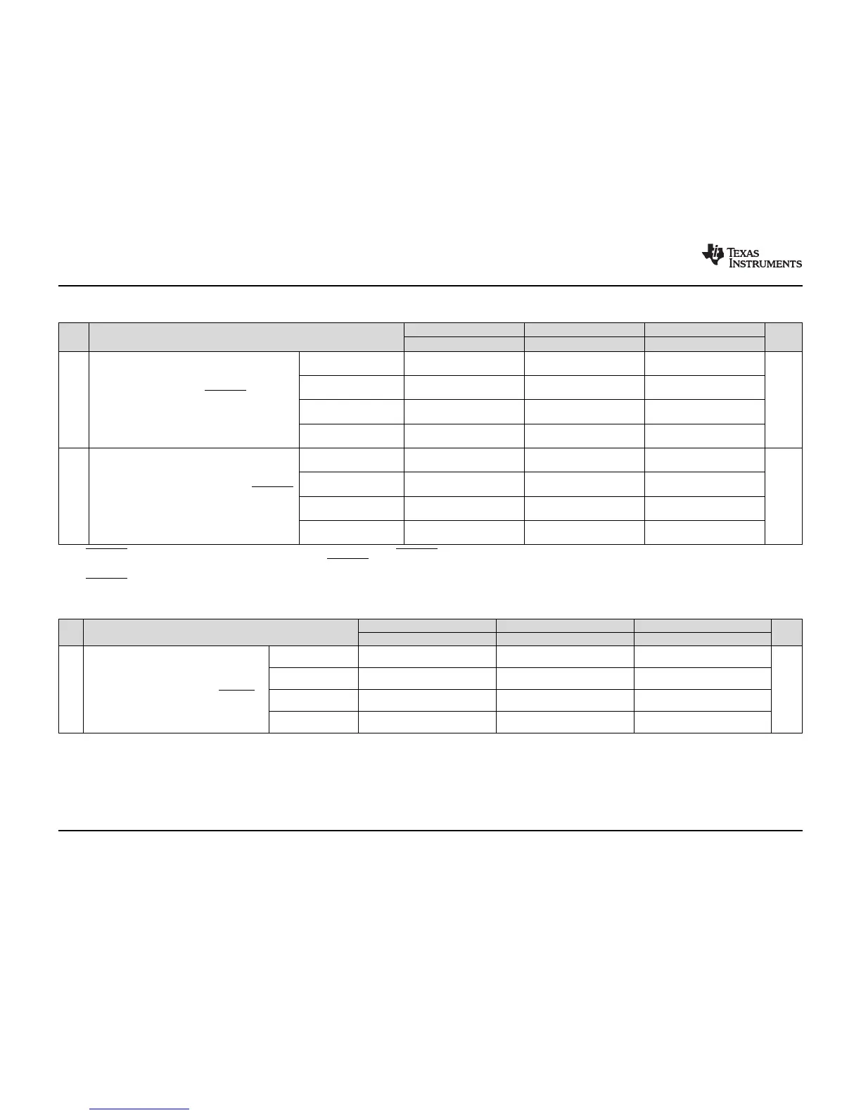
Table 6-72. Additional SPI0 Master Timings, 5-Pin Option
(1)(2)(3)
(continued)
1.3V, 1.2V 1.1V 1.0V
NO. PARAMETER UNIT
MIN MAX MIN MAX MIN MAX
Polarity = 0, Phase = 0,
2P-2 2P-2 2P-3
to SPI0_CLK rising
Polarity = 0, Phase = 1,
0.5M+2P-2 0.5M+2P-2 0.5M+2P-3
to SPI0_CLK rising
Delay from SPI0_SCS active to
22 t
d(SCS_SPC)M
ns
first SPI0_CLK
(7) (8) (9)
Polarity = 1, Phase = 0,
2P-2 2P-2 2P-3
to SPI0_CLK falling
Polarity = 1, Phase = 1,
0.5M+2P-2 0.5M+2P-2 0.5M+2P-3
to SPI0_CLK falling
Polarity = 0, Phase = 0,
3P+5 3P+5 3P+6
to SPI0_CLK rising
Polarity = 0, Phase = 1,
0.5M+3P+5 0.5M+3P+5 0.5M+3P+6
to SPI0_CLK rising
Delay from assertion of SPI0_ENA
23 t
d(ENA_SPC)M
ns
low to first SPI0_CLK edge.
(10)
Polarity = 1, Phase = 0,
3P+5 3P+5 3P+6
to SPI0_CLK falling
Polarity = 1, Phase = 1,
0.5M+3P+5 0.5M+3P+5 0.5M+3P+6
to SPI0_CLK falling
(7) If SPI0_ENA is asserted immediately such that the transmission is not delayed by SPI0_ENA.
(8) In the case where the master SPI is ready with new data before SPI0_SCS assertion.
(9) This delay can be increased under software control by the register bit field SPIDELAY.C2TDELAY[4:0].
(10) If SPI0_ENA was initially deasserted high and SPI0_CLK is delayed.
Table 6-73. Additional SPI0 Slave Timings, 4-Pin Enable Option
(1)(2)(3)
1.3V, 1.2V 1.1V 1.0V
NO. PARAMETER UNIT
MIN MAX MIN MAX MIN MAX
Polarity = 0, Phase = 0,
1.5P-3 2.5P+17.5 1.5P-3 2.5P+20 1.5P-3 2.5P+27
from SPI0_CLK falling
Polarity = 0, Phase = 1,
– 0.5M+1.5P-3 – 0.5M+2.5P+17.5 – 0.5M+1.5P-3 – 0.5M+2.5P+20 – 0.5M+1.5P-3 – 0.5M+2.5P+27
from SPI0_CLK falling
Delay from final SPI0_CLK edge
24 t
d(SPC_ENAH)S
ns
to slave deasserting SPI0_ENA.
Polarity = 1, Phase = 0,
1.5P-3 2.5P+17.5 1.5P-3 2.5P+20 1.5P-3 2.5P+27
from SPI0_CLK rising
Polarity = 1, Phase = 1,
– 0.5M+1.5P-3 – 0.5+2.5P+17.5 – 0.5M+1.5P-3 – 0.5+2.5P+20 – 0.5M+1.5P-3 – 0.5+2.5P+27
from SPI0_CLK rising
(1) These parameters are in addition to the general timings for SPI slave modes (Table 6-69).
(2) P = SYSCLK2 period; M = t
c(SPC)M
(SPI master bit clock period)
(3) Figure shows only Polarity = 0, Phase = 0 as an example. Table gives parameters for all four slave clocking modes.
158 Peripheral Information and Electrical Specifications Copyright © 2010–2014, Texas Instruments Incorporated
Submit Documentation Feedback
Product Folder Links: AM1808