AM1808
www.ti.com
SPRS653E –FEBRUARY 2010–REVISED MARCH 2014
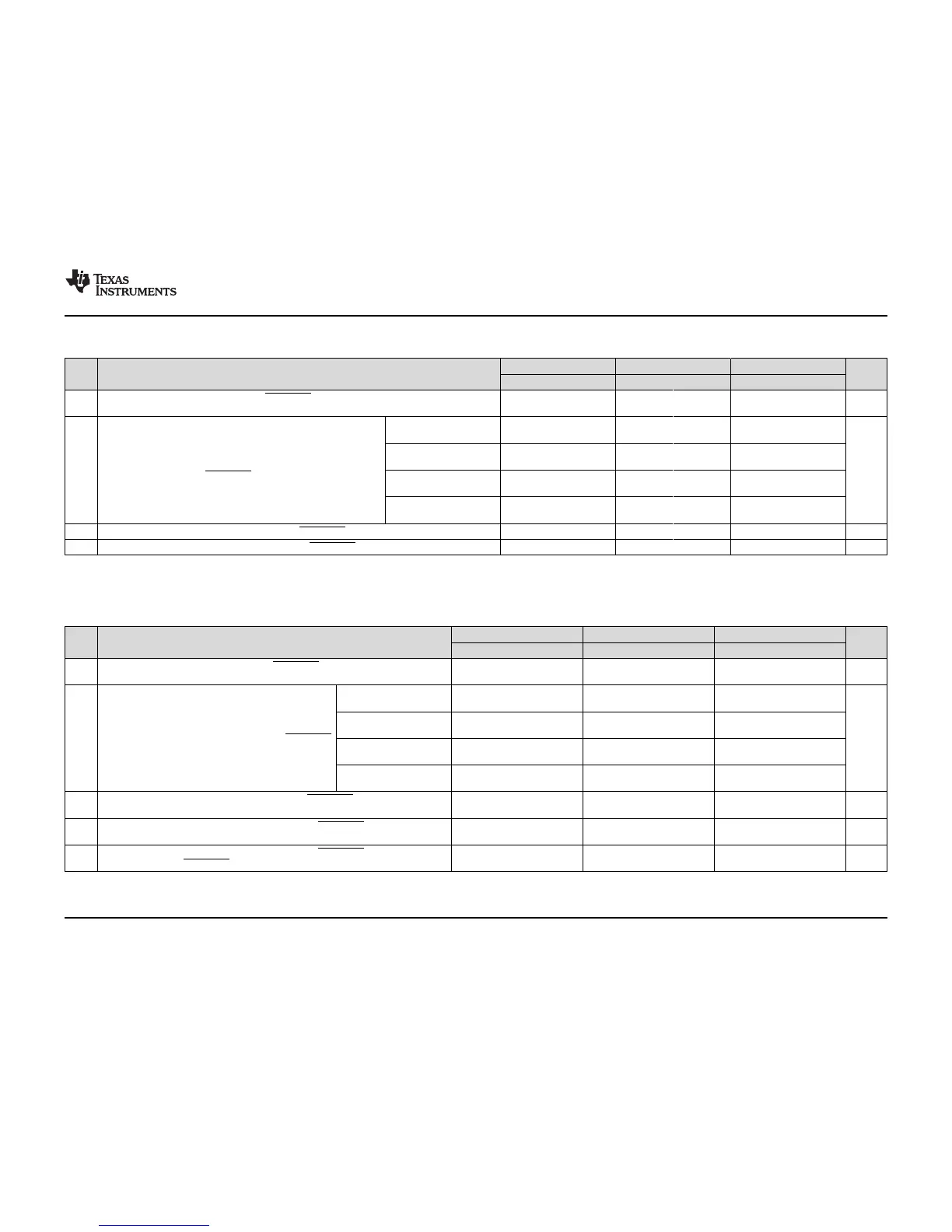
Table 6-74. Additional SPI0 Slave Timings, 4-Pin Chip Select Option
(1)(2)(3)
1.3V, 1.2V 1.1V 1.0V
NO. PARAMETER UNIT
MIN MAX MIN MAX MIN MAX
Required delay from SPI0_SCS asserted at slave to first SPI0_CLK edge
25 t
d(SCSL_SPC)S
P + 1.5 P + 1.5 P + 1.5 ns
at slave.
Polarity = 0, Phase = 0,
0.5M+P+4 0.5M+P+4 0.5M+P+5
from SPI0_CLK falling
Polarity = 0, Phase = 1,
P+4 P+4 P+5
from SPI0_CLK falling
Required delay from final SPI0_CLK edge
26 t
d(SPC_SCSH)S
ns
before SPI0_SCS is deasserted.
Polarity = 1, Phase = 0,
0.5M+P+4 0.5M+P+4 0.5M+P+5
from SPI0_CLK rising
Polarity = 1, Phase = 1,
P+4 P+4 P+5
from SPI0_CLK rising
27 t
ena(SCSL_SOMI)S
Delay from master asserting SPI0_SCS to slave driving SPI0_SOMI valid P+17.5 P+20 P+27 ns
28 t
dis(SCSH_SOMI)S
Delay from master deasserting SPI0_SCS to slave 3-stating SPI0_SOMI P+17.5 P+20 P+27 ns
(1) These parameters are in addition to the general timings for SPI slave modes (Table 6-69).
(2) P = SYSCLK2 period; M = t
c(SPC)M
(SPI master bit clock period)
(3) Figure shows only Polarity = 0, Phase = 0 as an example. Table gives parameters for all four slave clocking modes.
Table 6-75. Additional SPI0 Slave Timings, 5-Pin Option
(1)(2)(3)
1.3V, 1.2V 1.1V 1.0V
NO. PARAMETER UNIT
MIN MAX MIN MAX MIN MAX
Required delay from SPI0_SCS asserted at slave to first
25 t
d(SCSL_SPC)S
P + 1.5 P + 1.5 P + 1.5 ns
SPI0_CLK edge at slave.
Polarity = 0, Phase = 0,
0.5M+P+4 0.5M+P+4 0.5M+P+5
from SPI0_CLK falling
Polarity = 0, Phase = 1,
P+4 P+4 P+5
Required delay from final
from SPI0_CLK falling
26 t
d(SPC_SCSH)S
SPI0_CLK edge before SPI0_SCS ns
Polarity = 1, Phase = 0,
is deasserted.
0.5M+P+4 0.5M+P+4 0.5M+P+5
from SPI0_CLK rising
Polarity = 1, Phase = 1,
P+4 P+4 P+5
from SPI0_CLK rising
Delay from master asserting SPI0_SCS to slave driving
27 t
ena(SCSL_SOMI)S
P+17.5 P+20 P+27 ns
SPI0_SOMI valid
Delay from master deasserting SPI0_SCS to slave 3-stating
28 t
dis(SCSH_SOMI)S
P+17.5 P+20 P+27 ns
SPI0_SOMI
Delay from master deasserting SPI0_SCS to slave driving
29 t
ena(SCSL_ENA)S
17.5 20 27 ns
SPI0_ENA valid
(1) These parameters are in addition to the general timings for SPI slave modes (Table 6-69).
(2) P = SYSCLK2 period; M = t
c(SPC)M
(SPI master bit clock period)
(3) Figure shows only Polarity = 0, Phase = 0 as an example. Table gives parameters for all four slave clocking modes.
Copyright © 2010–2014, Texas Instruments Incorporated Peripheral Information and Electrical Specifications 159
Submit Documentation Feedback
Product Folder Links: AM1808