AM1808
www.ti.com
SPRS653E –FEBRUARY 2010–REVISED MARCH 2014
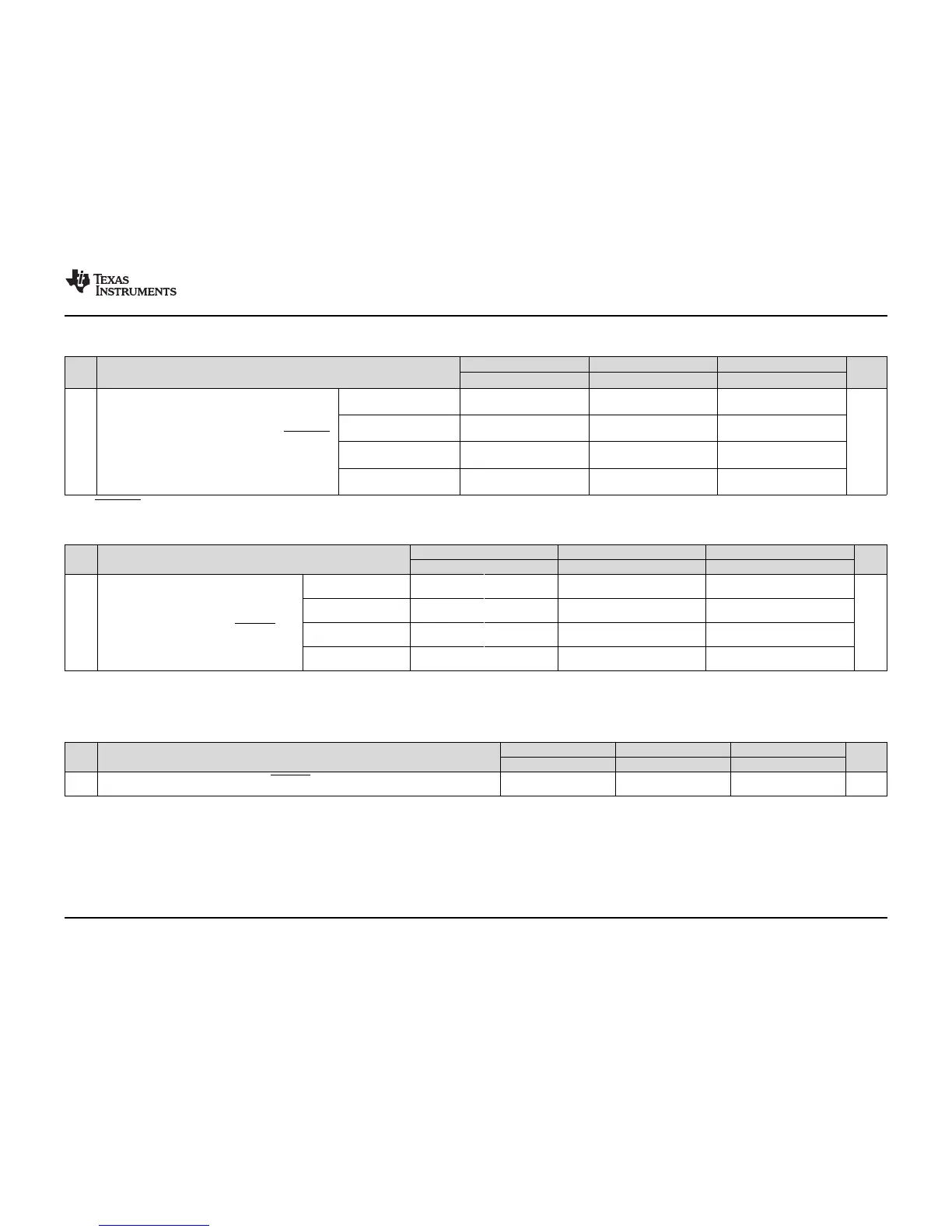
Table 6-80. Additional
(1)
SPI1 Master Timings, 5-Pin Option
(2)(3)
(continued)
1.3V, 1.2V 1.1V 1.0V
NO. PARAMETER UNIT
MIN MAX MIN MAX MIN MAX
Polarity = 0, Phase = 0,
3P+5 3P+5 3P+6
to SPI1_CLK rising
Polarity = 0, Phase = 1,
0.5M+3P+5 0.5M+3P+5 0.5M+3P+6
to SPI1_CLK rising
Delay from assertion of SPI1_ENA
23 t
d(ENA_SPC)M
ns
low to first SPI1_CLK edge.
(10)
Polarity = 1, Phase = 0,
3P+5 3P+5 3P+6
to SPI1_CLK falling
Polarity = 1, Phase = 1,
0.5M+3P+5 0.5M+3P+5 0.5M+3P+6
to SPI1_CLK falling
(10) If SPI1_ENA was initially deasserted high and SPI1_CLK is delayed.
Table 6-81. Additional
(1)
SPI1 Slave Timings, 4-Pin Enable Option
(2)(3)
1.3V, 1.2V 1.1V 1.0V
NO. PARAMETER UNIT
MIN MAX MIN MAX MIN MAX
Polarity = 0, Phase = 0,
1.5P-3 2.5P+15 1.5P-10 2.5P+17 1.5P-12 2.5P+19
from SPI1_CLK falling
Polarity = 0, Phase = 1,
–0.5M+1.5P-3 –0.5M+2.5P+15 –0.5M+1.5P-10 –0.5M+2.5P+17 –0.5M+1.5P-12 –0.5M+2.5P+19
from SPI1_CLK falling
Delay from final SPI1_CLK edge to
24 t
d(SPC_ENAH)S
ns
slave deasserting SPI1_ENA.
Polarity = 1, Phase = 0,
1.5P-3 2.5P+15 1.5P-10 2.5P+17 1.5P-12 2.5P+19
from SPI1_CLK rising
Polarity = 1, Phase = 1,
–0.5M+1.5P-3 –0.5M+2.5P+15 –0.5M+1.5P-10 –0.5M+2.5P+17 –0.5M+1.5P-12 –0.5M+2.5P+19
from SPI1_CLK rising
(1) These parameters are in addition to the general timings for SPI slave modes (Table 6-77).
(2) P = SYSCLK2 period; M = t
c(SPC)M
(SPI master bit clock period)
(3) Figure shows only Polarity = 0, Phase = 0 as an example. Table gives parameters for all four slave clocking modes.
Table 6-82. Additional
(1)
SPI1 Slave Timings, 4-Pin Chip Select Option
(2)(3)
1.3V, 1.2V 1.1V 1.0V
NO. PARAMETER UNIT
MIN MAX MIN MAX MIN MAX
Required delay from SPI1_SCS asserted at slave to first SPI1_CLK edge at
25 t
d(SCSL_SPC)S
P+1.5 P+1.5 P+1.5 ns
slave.
(1) These parameters are in addition to the general timings for SPI slave modes (Table 6-77).
(2) P = SYSCLK2 period; M = t
c(SPC)M
(SPI master bit clock period)
(3) Figure shows only Polarity = 0, Phase = 0 as an example. Table gives parameters for all four slave clocking modes.
Copyright © 2010–2014, Texas Instruments Incorporated Peripheral Information and Electrical Specifications 165
Submit Documentation Feedback
Product Folder Links: AM1808
 Loading...