TMS320 SECOND GENERATION
DIGITAL SIGNAL PROCESSORS
SPRS010B — MAY 1987 — REVISED NOVEMBER 1990
POST OFFICE BOX 1443 HOUSTON, TEXAS 77001
30
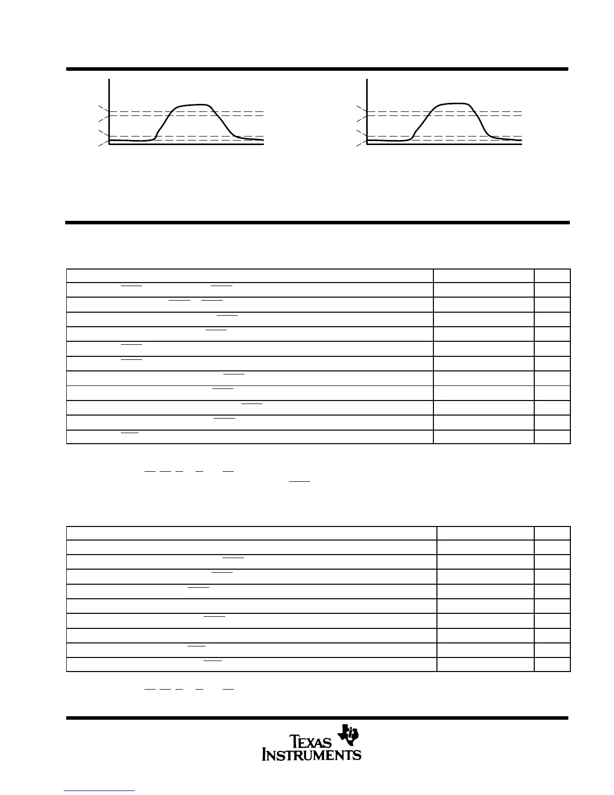
0.80 V
0.92 V
1.88 V
2.0 V
0
V
IH
(Min)
V
IL
(Max)
(a) Input
0.6 V
0.8 V
2.2 V
2.4 V
0
V
OH
(Min)
V
OL
(Max)
(b) Output
Figure 5. Voltage Reference Levels
MEMORY AND PERIPHERAL INTERFACE TIMING
switching characteristics over recommended operating conditions (see Note 3)
PARAMETER MIN TYP MAX UNIT
t
d(C1-S)
STRB from CLKOUT1 (if STRB is present) Q--6 Q Q+6 ns
t
d(C2-S)
CLKOUT2 to STRB (if STRB is present) -- 6 0 6 ns
t
su(A)
Address setup time before STRB low(seeNote5) Q--12 ns
t
h(A)
Address hold time after STRB high (see Note 5) Q--8 ns
t
w(SL)
STRB low pulse duration (no wait states, see Note 6) 2Q -- 5 2Q + 5 ns
t
w(SH)
STRB high pulse duration (between consecutive cycles, see Note 6) 2Q -- 5 2Q + 5 ns
t
su(D)W
Data write setup time before STRB high (no wait s tates) 2Q -- 20 ns
t
h(D)W
DatawriteholdtimefromSTRBhigh Q--10 Q ns
t
en(D)
Data bus starts being driven after STRB low (write cycle) 0
†
ns
t
dis(D)
Data bus three-state after STRB high (write cycle) Q Q+15
†
ns
t
d(MSC)
MSC valid from CLKOUT1 -- 1 2 0 12 ns
†
Value derived from characterization data and not tested.
NOTES: 3. Q = 1/4t
c(C)
.
5. A15-A0, PS
,DS,IS,R/W, and BR timings are all included in timings referenced as “address”.
6. Delays between CLKOUT1/CLKOUT2 edges and STRB
edges track each other, resulting in t
w(SL)
and t
w(SH)
being 2Q with no wait
states.
timing requirements over recommended operating conditions (see Note 3)
MIN NOM MAX UNIT
t
a(A)
Read data access time from address time (read cycle, see Notes 5 and 7) 3Q -- 35 ns
t
su(D)R
Data read setup time before STRB high 23 ns
t
h(D)R
Data read hold time from S TRB high 0 ns
t
d(SL-R)
READY valid after STRB low (no wait states) Q--20 ns
t
d(C2H-R)
READY valid after CLKOUT2 high Q--20 ns
t
h(SL-R)
READYholdtimeafterSTRBlow (no wait states) Q+3 ns
t
h(C2H-R)
READY hold after CLKOUT2 high Q+3 ns
t
d(M-R)
READY v alid after MSC valid 2Q -- 25 ns
t
h(M-R)
READY hold time after MSC valid 0 ns
NOTES: 3. Q = 1/4t
c(C)
.
5. A15-A0, PS
,DS,IS,R/W, and BR timings are all included in timings referenced as “address”.
7. Read data access time is defines as t
a(A)
=t
su(A)
+t
w(SL)
-- t
su(D)R
.
ADVANCE INFORMATION

 Loading...