SARA-R4 series - System integration manual
UBX-16029218 - R20 System description Page 12 of 128
C1-Public
SARA-R4 series modules internally consist of the following sections described herein with more
details than the simplified block diagrams of Figure 1, Figure 2 and Figure 3.
RF section
The RF section is composed of the following main elements:
• RF switch connecting the antenna port (ANT) to the suitable RF Tx / Rx paths for LTE Cat M1 /
NB-IoT Half-Duplex operations
• Power Amplifiers (PA) amplifying the Tx signal modulated and pre-amplified by the RF transceiver
• RF filters along the Tx and Rx signal paths providing RF filtering
• RF transceiver, performing modulation, up-conversion and pre-amplification of the baseband
signals for LTE transmission, and performing down-conversion and demodulation of the RF signal
for LTE reception
• 19.2 MHz Temperature-Controlled Crystal Oscillator (TCXO) generating the reference clock signal
for the RF transceiver and the baseband system, when the related system is in active mode or
connected mode.
Baseband and power management section
The baseband and power management section, is composed of the following main elements:
• On-chip modem processor, vector signal processor, with dedicated hardware assistance for signal
processing and system timing
• On-chip modem processor, with interfaces control functions
• On-chip voltage regulators to derive all the internal or external (V_SIM, V_INT) supply voltages
from the module supply input VCC
• Dedicated flash memory IC
• 32.768 kHz crystal oscillator to provide the clock reference in the low power idle mode, which can
be enabled using the +UPSV AT command, and in the PSM deep-sleep mode, which can be enabled
using the +CPSMS AT command
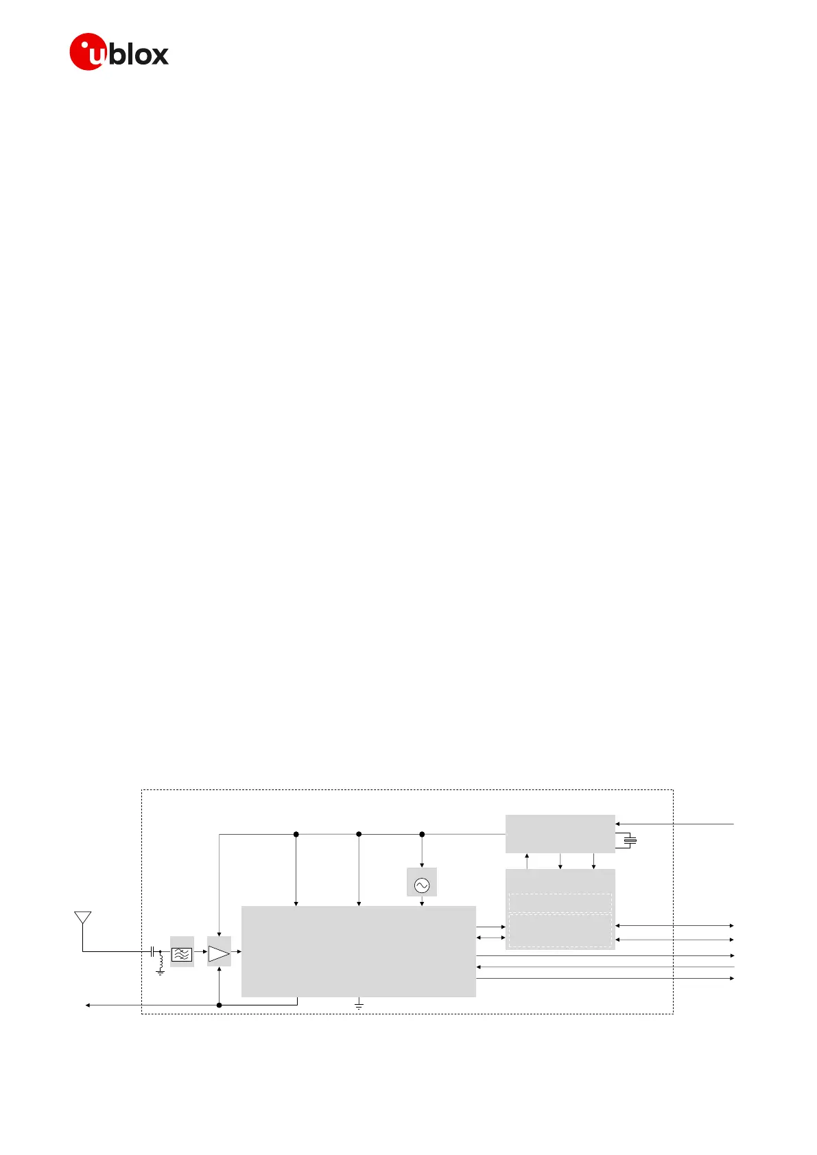
GNSS section (SARA-R422M8S modules only)
The GNSS section, is composed of the following main elements illustrated in Figure 4:
• u-blox UBX-M8030-CT concurrent GNSS chipset with SPG 3.01 firmware version
• Dedicated SAW filter
• Additional Low Noise Amplifier (LNA)
• 26 MHz Temperature-Controlled Crystal Oscillator (TCXO) generating the reference clock signal
for the GNSS system
 Loading...