SARA-R4 series - System integration manual
UBX-16029218 - R20 Design-in Page 81 of 128
C1-Public
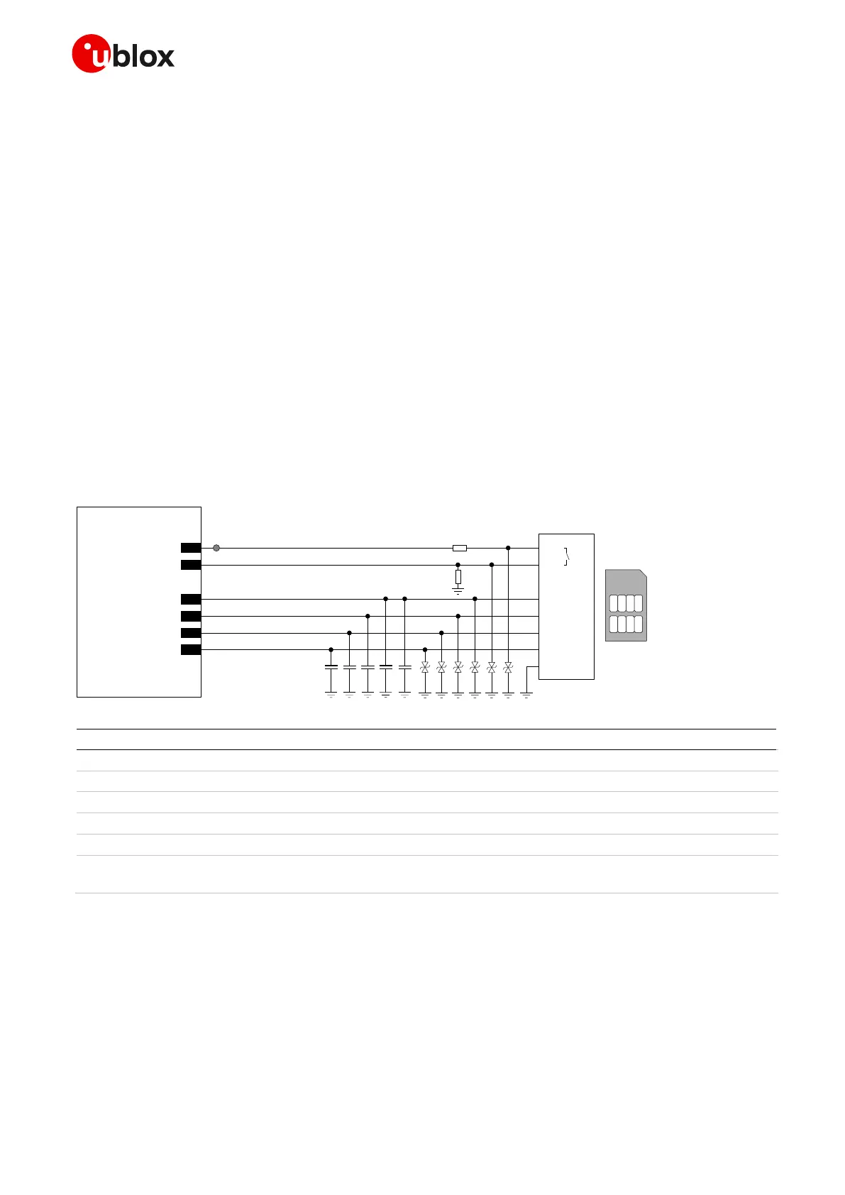
• Connect one pin of the normally-open mechanical switch integrated in the SIM connector (as the
SW2 pin in Figure 50) to the GPIO5 input pin, providing a weak pull-down resistor (e.g. 470 k, as
R2 in Figure 50).
• Connect the other pin of the normally-open mechanical switch integrated in the SIM connector
(SW1 pin in Figure 50) to V_INT 1.8 V supply output by means of a strong pull-up resistor (e.g.
1 k, as R1 in Figure 50)
• Provide a 100 nF bypass capacitor (e.g. Murata GRM155R71C104K) at the SIM supply line (VSIM),
close to the related pad of the SIM connector, to prevent digital noise.
• Provide a bypass capacitor of about 22 pF to 47 pF (e.g. Murata GRM1555C1H470J) on each SIM
line (VSIM, SIM_CLK, SIM_IO, SIM_RST), very close to each related pad of the SIM connector, to
prevent RF coupling especially in case the RF antenna is placed closer than 10 - 30 cm from the
SIM card holder.
• Provide a low capacitance (i.e. less than 10 pF) ESD protection (e.g. Tyco Electronics
PESD0402-140) on each externally accessible SIM line, close to each related pad of the SIM
connector. The ESD sensitivity rating of SIM interface pins is 1 kV (HBM according to
JESD22-A114), so that, according to the EMC/ESD requirements of the custom application,
higher protection level can be required if the lines are externally accessible.
• Limit capacitance and series resistance on each SIM signal to match the requirements for the SIM
interface (18.7 ns = maximum rise time on SIM_CLK, 1.0 µs = maximum rise time on SIM_IO and
SIM_RST).
 Loading...