VIA Technologies, Inc.
VT82C42
-6-
6. VT82C42 Signal Description
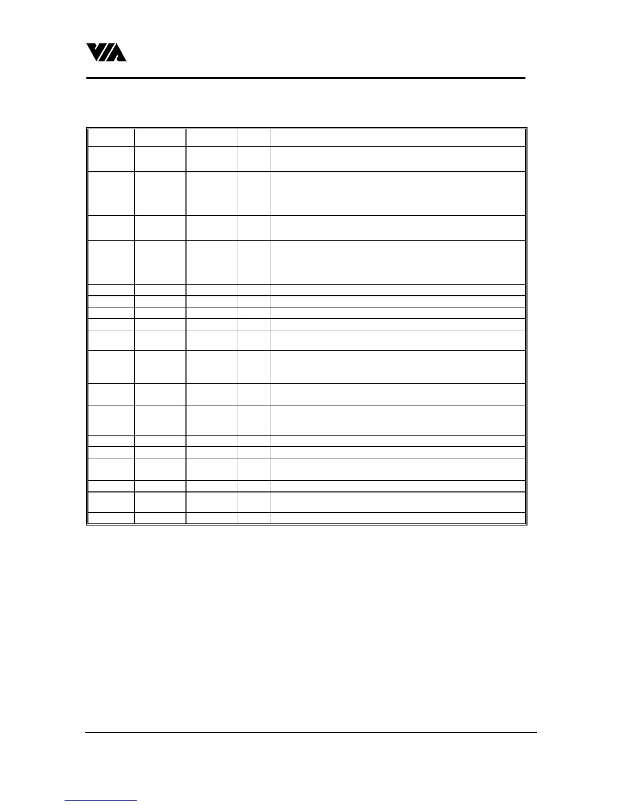
Table 4. Signal Description for VT82C42
Symbol 40-Pin 44-Pin Type Name and Function
D
0
-D
7
(BUS)
12-19 14-20 I/O Act as data input or data output.
P
10
-P
13
27-30 30-33 I/O Pullup open drain port. Writing a '1' to these ports tri-states the
ports. Act as input 'high' simultaneously if no outside 'low'
connection. Writing a '0' to these ports results in generating a low
on the port.
P
20
-P
27
21-24
35-38
24-27
39-42
O
Output Port 20 - Output Port 23
Output Port 24 - Output Port 27
P
14
-P
15
31, 32 35, 36 I/O Pullup open drain port. Writing a '1' to these ports tri-states the
ports. Act as input 'high' simultaneously if no outside 'low'
connection. Writing a '0' to these ports results in generating a low
on the port.
P
16
-P
17
33, 34 37, 38 I Input port 16, Input port 17
WR# 10 11 I Act as a write signal.
RD# 8 9 I Act as a read signal.
CS# 6 7 I Chip select of this chip.
A
0
9 10 I Command/Data select when RD# or WR# is active.
TEST 0,
TEST 1
1
39
2
43
I Act as Keyboard clock input in both AT mode & PS2 mode
Act as Keyboard Data input in AT mode. Act as Mouse Clock
input in PS2 mode.
XTAL 1,
XTAL 2
2
3
3
4
I Act as clock input to the chips. Can be connected to LC circuit or
a single clock source (X2).
TH_SS
TH_PROG
TH_SSPP
5
25
26
6
28
29
I Tie to VCC
TL_EA 7 8 I Tie to ground.
SYNC 11 12 O Internal state synchronous output.
NC 1, 13, 23,
34
I No connection.
RESET# 4 5 I A low in this pin reset the chip to a known state.
V
CC
40 44 Power supply of 4.5 to 5.5v.
GND 20 22 Ground.
1. Description for Table 4
RESET# is active low and is only an input pin. VT82C42 requires 10 clocks before RESET# goes to high to
have the chip go to a known state.
Pins WR#, RD#, CS# and A
o
are all input only pins and must activate for at least one clock cycle width to be
recognised by the VT82C42.
D
0
-d
7
are two-way pins, each having 4mA TTL compatible output driving. When D
0
-D
7
is provided by the
host, write cycle data should cover all the WR# CS# A
0
command width. When the D
0
-D
7
is provided by the
VT82C42, the D
0
-D
7
is available as long as the RD#=0 CS#=0 command is asserted and is held one clock
cycle after the command is deasserted.
TEST0,TEST1 are input only pins. TEST0 is expected to connect to KBCLK no matter what mode the
VT82C42 is in. TEST1 is expected to connect to KBDATA when in AT-mode, and is expected to connect to
MSCLK when in PS/2 mode. They have a 50K ohm pull up internally.
 Loading...