VIA Technologies, Inc.
VT82C42
-7-
P16,P17 are input only pins. They have a 50K ohm pull up internally.
P20-P26 are all output only pins, each has 4mA TTL-compatible output. P27 is also output only pin, but with
16mA TTL-compatible output.
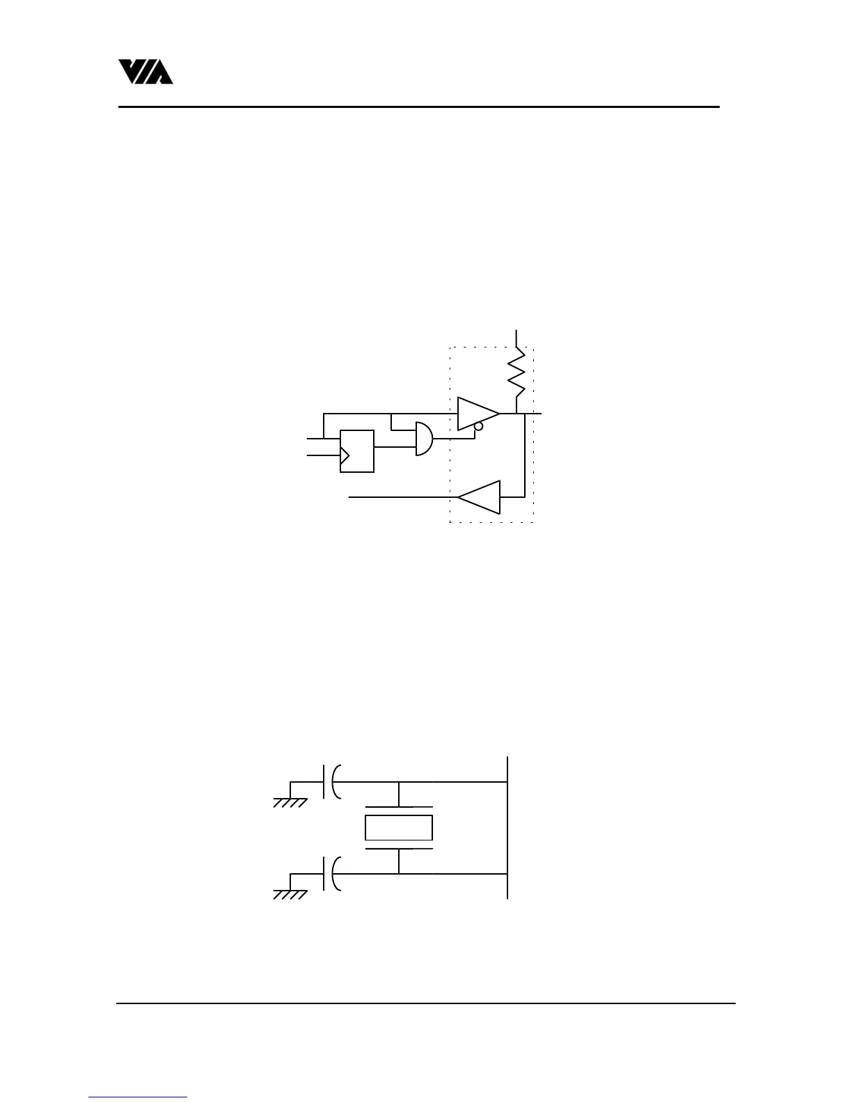
For two-way port pins, P
10
-P
15
, when floated (by written "1" to the port), the signals from these pins are all
sustained tri-state output. That means when it is to be floated high, it will be driven high for one 8Mhz cycle
before goes to float. The external connection is suggested to have a 4.7K pull-up resistor to maintain high after
floating. The following logic diagram shows the corresponding functions. Note that the part surrounded by
dash lines is a bi-directional TTL-compatible output with 4mA driving capabilities.
CLOCK
P10O
P10I
P10
VCC
50K ohm
Fig 4.
TH_SS, TH_PROG and TH_SSPP are all input pins, and must be tied to high for normal operation. TL_EA is
an input pin, and must be tied to low for normal operation.
SYNC is output pin, which drives some internal states out, this pin is only useful when in debugging stage. For
normal operation, it should leave opened.
MSLKMD is the mouse lock enable pin. When this pin is tied low, the Mouse Lock mode is enabled,
otherwise the Mouse Lock mode is disabled.
XTAL1, XTAL2 is the clocking source input of VT82C42, it can be implemented as in the figure 5. or figure
6. underneath:
20pf
20pf
1 - 12 MHz
XTAL1
XTAL2
Figure 5. Crystal Connections for Clock source for VT82C42